稳健的低于100 纳米 采用多步骤开发的T型门制造工艺

IF 2.8 Q2 ENGINEERING, ELECTRICAL & ELECTRONIC
Kaivan Karami , Aniket Dhongde , Huihua Cheng , Paul M. Reynolds , Bojja Aditya Reddy , Daniel Ritter , Chong Li , Edward Wasige , Stephen Thoms
{"title":"稳健的低于100 纳米 采用多步骤开发的T型门制造工艺","authors":"Kaivan Karami ,&nbsp;Aniket Dhongde ,&nbsp;Huihua Cheng ,&nbsp;Paul M. Reynolds ,&nbsp;Bojja Aditya Reddy ,&nbsp;Daniel Ritter ,&nbsp;Chong Li ,&nbsp;Edward Wasige ,&nbsp;Stephen Thoms","doi":"10.1016/j.mne.2023.100211","DOIUrl":null,"url":null,"abstract":"<div><p>We demonstrate the fabrication of sub-100 nm T-Gate structures using a single electron beam lithography exposure and a tri-layer resist stack - PMMA/LOR/CSAR. Recent developments in modelling resist development were used to design the process, in which each resist is developed separately to optimise the resulting structure. By using a modelling approach and proximity correcting for the full resist stack, we were able to independently vary gate length (50-100 nm) and head size (250-500 nm) at the design stage and fabricate these T-Gates with high yield.</p></div>","PeriodicalId":37111,"journal":{"name":"Micro and Nano Engineering","volume":null,"pages":null},"PeriodicalIF":2.8000,"publicationDate":"2023-06-01","publicationTypes":"Journal Article","fieldsOfStudy":null,"isOpenAccess":false,"openAccessPdf":"","citationCount":"0","resultStr":"{\"title\":\"Robust sub-100 nm T-Gate fabrication process using multi-step development\",\"authors\":\"Kaivan Karami ,&nbsp;Aniket Dhongde ,&nbsp;Huihua Cheng ,&nbsp;Paul M. Reynolds ,&nbsp;Bojja Aditya Reddy ,&nbsp;Daniel Ritter ,&nbsp;Chong Li ,&nbsp;Edward Wasige ,&nbsp;Stephen Thoms\",\"doi\":\"10.1016/j.mne.2023.100211\",\"DOIUrl\":null,\"url\":null,\"abstract\":\"<div><p>We demonstrate the fabrication of sub-100 nm T-Gate structures using a single electron beam lithography exposure and a tri-layer resist stack - PMMA/LOR/CSAR. Recent developments in modelling resist development were used to design the process, in which each resist is developed separately to optimise the resulting structure. By using a modelling approach and proximity correcting for the full resist stack, we were able to independently vary gate length (50-100 nm) and head size (250-500 nm) at the design stage and fabricate these T-Gates with high yield.</p></div>\",\"PeriodicalId\":37111,\"journal\":{\"name\":\"Micro and Nano Engineering\",\"volume\":null,\"pages\":null},\"PeriodicalIF\":2.8000,\"publicationDate\":\"2023-06-01\",\"publicationTypes\":\"Journal Article\",\"fieldsOfStudy\":null,\"isOpenAccess\":false,\"openAccessPdf\":\"\",\"citationCount\":\"0\",\"resultStr\":null,\"platform\":\"Semanticscholar\",\"paperid\":null,\"PeriodicalName\":\"Micro and Nano Engineering\",\"FirstCategoryId\":\"1085\",\"ListUrlMain\":\"https://www.sciencedirect.com/science/article/pii/S2590007223000412\",\"RegionNum\":0,\"RegionCategory\":null,\"ArticlePicture\":[],\"TitleCN\":null,\"AbstractTextCN\":null,\"PMCID\":null,\"EPubDate\":\"\",\"PubModel\":\"\",\"JCR\":\"Q2\",\"JCRName\":\"ENGINEERING, ELECTRICAL & ELECTRONIC\",\"Score\":null,\"Total\":0}","platform":"Semanticscholar","paperid":null,"PeriodicalName":"Micro and Nano Engineering","FirstCategoryId":"1085","ListUrlMain":"https://www.sciencedirect.com/science/article/pii/S2590007223000412","RegionNum":0,"RegionCategory":null,"ArticlePicture":[],"TitleCN":null,"AbstractTextCN":null,"PMCID":null,"EPubDate":"","PubModel":"","JCR":"Q2","JCRName":"ENGINEERING, ELECTRICAL & ELECTRONIC","Score":null,"Total":0}
引用次数: 0

摘要

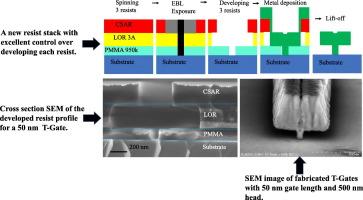
我们展示了使用单电子束光刻曝光和三层抗蚀剂堆叠PMMA/LOR/CSAR制造亚100nm T型栅极结构。抗蚀剂开发模型的最新发展被用于设计工艺,其中每个抗蚀剂都被单独开发,以优化最终的结构。通过对全抗蚀剂堆叠使用建模方法和接近校正,我们能够在设计阶段独立地改变栅极长度(50-100nm)和磁头尺寸(250-500nm),并以高产率制造这些T型门。
本文章由计算机程序翻译,如有差异,请以英文原文为准。

Robust sub-100 nm T-Gate fabrication process using multi-step development

Robust sub-100 nm T-Gate fabrication process using multi-step development

We demonstrate the fabrication of sub-100 nm T-Gate structures using a single electron beam lithography exposure and a tri-layer resist stack - PMMA/LOR/CSAR. Recent developments in modelling resist development were used to design the process, in which each resist is developed separately to optimise the resulting structure. By using a modelling approach and proximity correcting for the full resist stack, we were able to independently vary gate length (50-100 nm) and head size (250-500 nm) at the design stage and fabricate these T-Gates with high yield.

求助全文
通过发布文献求助,成功后即可免费获取论文全文。 去求助
来源期刊
Micro and Nano Engineering
Micro and Nano Engineering Engineering-Electrical and Electronic Engineering
CiteScore
3.30
自引率
0.00%
发文量
67
审稿时长
80 days
×
引用
GB/T 7714-2015
复制
MLA
复制
APA
复制
导出至
BibTeX EndNote RefMan NoteFirst NoteExpress
×
提示
您的信息不完整,为了账户安全,请先补充。
现在去补充
×
提示
您因"违规操作"
具体请查看互助需知
我知道了
×
提示
确定
请完成安全验证×
copy
已复制链接
快去分享给好友吧!
我知道了
右上角分享
点击右上角分享
0
联系我们:info@booksci.cn Book学术提供免费学术资源搜索服务,方便国内外学者检索中英文文献。致力于提供最便捷和优质的服务体验。 Copyright © 2023 布克学术 All rights reserved.
京ICP备2023020795号-1
ghs 京公网安备 11010802042870号
Book学术文献互助
Book学术文献互助群
群 号:481959085
Book学术官方微信