{"title":"Ru/Ta双分子层方法用于EUV掩膜吸收:实验模式和模拟成像视角","authors":"Devesh Thakare , Jean-François de Marneffe , Annelies Delabie , Vicky Philipsen","doi":"10.1016/j.mne.2023.100223","DOIUrl":null,"url":null,"abstract":"<div><p>The optical properties and geometry of EUV mask absorbers play an essential role in determining the imaging performance of a mask in EUV lithography. Imaging metrics, including Normalized Image Log Slope (NILS), Telecentricity Error (TCE), and Best Focus Variation (BFV) through pitch deteriorate because of Mask 3-Dimensional (M3D) effects in EUV lithography, which limits the production efficiency. Alternative absorbers, including alloys of Ru and Ta, are anticipated to reduce some of the M3D effects; however, patterning these materials is challenging due to their low etch rates and poor etch selectivity against the Ru mask capping layer. Therefore, we propose a Ru/Ta bilayer approach to EUV mask absorbers and investigate it from a patterning and imaging standpoint. The top Ru layer thickness is calculated using the thin film interference phenomena, and we determine the bottom Ta layer that can produce improved NILS by utilizing the total absorber thickness optimization methodology. We demonstrate the patterning of the Ru/Ta bilayer using a two-step etch; the top Ru layer is patterned with Cl<sub>2</sub>-O<sub>2</sub> Reactive Ion Etch (RIE), and the bottom Ta layer with Cl<sub>2</sub>-N<sub>2</sub> RIE. The geometry and morphology of the patterned bilayer stack are investigated using TEM (Transmission Electron Microscopy), and interdiffusion at the interface of Ru and Ta is studied using EDS-STEM (Energy Dispersive X-ray Spectroscopy-Scanning Transmission Electron Microscopy). The non-ideal traits of the Ru/Ta bilayer stack, determined by experimental characterization techniques, are used to simulate the imaging performance and then compared against an ideal Ru/Ta bilayer stack, along with the reference Ta-based absorber. Even when non-idealities are considered, the simulation findings demonstrate that the Ru/Ta bilayer absorber exhibits improved NILS and reduced BFV compared to the Ta-based absorber. The outcomes encourage further research into the possibilities of multilayer absorbers, to tailor their optical characteristics by varying the thickness of individual layers.</p></div>","PeriodicalId":37111,"journal":{"name":"Micro and Nano Engineering","volume":"20 ","pages":"Article 100223"},"PeriodicalIF":2.8000,"publicationDate":"2023-09-01","publicationTypes":"Journal Article","fieldsOfStudy":null,"isOpenAccess":false,"openAccessPdf":"","citationCount":"0","resultStr":"{\"title\":\"Ru/Ta bilayer approach to EUV mask absorbers: Experimental patterning and simulated imaging perspective\",\"authors\":\"Devesh Thakare , Jean-François de Marneffe , Annelies Delabie , Vicky Philipsen\",\"doi\":\"10.1016/j.mne.2023.100223\",\"DOIUrl\":null,\"url\":null,\"abstract\":\"<div><p>The optical properties and geometry of EUV mask absorbers play an essential role in determining the imaging performance of a mask in EUV lithography. Imaging metrics, including Normalized Image Log Slope (NILS), Telecentricity Error (TCE), and Best Focus Variation (BFV) through pitch deteriorate because of Mask 3-Dimensional (M3D) effects in EUV lithography, which limits the production efficiency. Alternative absorbers, including alloys of Ru and Ta, are anticipated to reduce some of the M3D effects; however, patterning these materials is challenging due to their low etch rates and poor etch selectivity against the Ru mask capping layer. Therefore, we propose a Ru/Ta bilayer approach to EUV mask absorbers and investigate it from a patterning and imaging standpoint. The top Ru layer thickness is calculated using the thin film interference phenomena, and we determine the bottom Ta layer that can produce improved NILS by utilizing the total absorber thickness optimization methodology. We demonstrate the patterning of the Ru/Ta bilayer using a two-step etch; the top Ru layer is patterned with Cl<sub>2</sub>-O<sub>2</sub> Reactive Ion Etch (RIE), and the bottom Ta layer with Cl<sub>2</sub>-N<sub>2</sub> RIE. The geometry and morphology of the patterned bilayer stack are investigated using TEM (Transmission Electron Microscopy), and interdiffusion at the interface of Ru and Ta is studied using EDS-STEM (Energy Dispersive X-ray Spectroscopy-Scanning Transmission Electron Microscopy). The non-ideal traits of the Ru/Ta bilayer stack, determined by experimental characterization techniques, are used to simulate the imaging performance and then compared against an ideal Ru/Ta bilayer stack, along with the reference Ta-based absorber. Even when non-idealities are considered, the simulation findings demonstrate that the Ru/Ta bilayer absorber exhibits improved NILS and reduced BFV compared to the Ta-based absorber. The outcomes encourage further research into the possibilities of multilayer absorbers, to tailor their optical characteristics by varying the thickness of individual layers.</p></div>\",\"PeriodicalId\":37111,\"journal\":{\"name\":\"Micro and Nano Engineering\",\"volume\":\"20 \",\"pages\":\"Article 100223\"},\"PeriodicalIF\":2.8000,\"publicationDate\":\"2023-09-01\",\"publicationTypes\":\"Journal Article\",\"fieldsOfStudy\":null,\"isOpenAccess\":false,\"openAccessPdf\":\"\",\"citationCount\":\"0\",\"resultStr\":null,\"platform\":\"Semanticscholar\",\"paperid\":null,\"PeriodicalName\":\"Micro and Nano Engineering\",\"FirstCategoryId\":\"1085\",\"ListUrlMain\":\"https://www.sciencedirect.com/science/article/pii/S2590007223000539\",\"RegionNum\":0,\"RegionCategory\":null,\"ArticlePicture\":[],\"TitleCN\":null,\"AbstractTextCN\":null,\"PMCID\":null,\"EPubDate\":\"\",\"PubModel\":\"\",\"JCR\":\"Q2\",\"JCRName\":\"ENGINEERING, ELECTRICAL & ELECTRONIC\",\"Score\":null,\"Total\":0}","platform":"Semanticscholar","paperid":null,"PeriodicalName":"Micro and Nano Engineering","FirstCategoryId":"1085","ListUrlMain":"https://www.sciencedirect.com/science/article/pii/S2590007223000539","RegionNum":0,"RegionCategory":null,"ArticlePicture":[],"TitleCN":null,"AbstractTextCN":null,"PMCID":null,"EPubDate":"","PubModel":"","JCR":"Q2","JCRName":"ENGINEERING, ELECTRICAL & ELECTRONIC","Score":null,"Total":0}
引用次数: 0
摘要
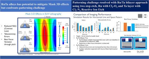
EUV掩模吸收体的光学性质和几何形状在决定EUV光刻中掩模的成像性能方面起着至关重要的作用。由于EUV光刻中的掩模三维(M3D)效应,包括归一化图像对数斜率(NILS)、远心误差(TCE)和通过间距的最佳聚焦变化(BFV)在内的成像指标恶化,这限制了生产效率。替代吸收剂,包括Ru和Ta的合金,预计将减少一些M3D效应;然而,图案化这些材料是具有挑战性的,因为它们的蚀刻速率低并且对Ru掩模覆盖层的蚀刻选择性差。因此,我们提出了一种用于EUV掩模吸收体的Ru/Ta双层方法,并从图案化和成像的角度对其进行了研究。利用薄膜干涉现象计算了顶部Ru层的厚度,并利用总吸收层厚度优化方法确定了可以产生改进NILS的底部Ta层。我们展示了使用两步蚀刻来图案化Ru/Ta双层;顶部Ru层用Cl2-O2反应离子蚀刻(RIE)图案化并且底部Ta层用Cl1-N2 RIE图案化。使用TEM(透射电子显微镜)研究了图案化双层堆叠的几何结构和形态,并使用EDS-STEM(能量分散X射线光谱扫描透射电子显微镜(Energy Dispersive X-ray Spectroscopy Scanning Transmission Electron Microscopy))研究了Ru和Ta界面处的相互扩散。通过实验表征技术确定的Ru/Ta双层堆叠的非理想特性用于模拟成像性能,然后与理想Ru/Ta单层堆叠以及参考Ta基吸收体进行比较。即使考虑了非理想性,模拟结果也表明,与Ta基吸收体相比,Ru/Ta双层吸收体表现出改进的NILS和降低的BFV。这些结果鼓励进一步研究多层吸收体的可能性,通过改变单个层的厚度来调整其光学特性。
Ru/Ta bilayer approach to EUV mask absorbers: Experimental patterning and simulated imaging perspective
The optical properties and geometry of EUV mask absorbers play an essential role in determining the imaging performance of a mask in EUV lithography. Imaging metrics, including Normalized Image Log Slope (NILS), Telecentricity Error (TCE), and Best Focus Variation (BFV) through pitch deteriorate because of Mask 3-Dimensional (M3D) effects in EUV lithography, which limits the production efficiency. Alternative absorbers, including alloys of Ru and Ta, are anticipated to reduce some of the M3D effects; however, patterning these materials is challenging due to their low etch rates and poor etch selectivity against the Ru mask capping layer. Therefore, we propose a Ru/Ta bilayer approach to EUV mask absorbers and investigate it from a patterning and imaging standpoint. The top Ru layer thickness is calculated using the thin film interference phenomena, and we determine the bottom Ta layer that can produce improved NILS by utilizing the total absorber thickness optimization methodology. We demonstrate the patterning of the Ru/Ta bilayer using a two-step etch; the top Ru layer is patterned with Cl2-O2 Reactive Ion Etch (RIE), and the bottom Ta layer with Cl2-N2 RIE. The geometry and morphology of the patterned bilayer stack are investigated using TEM (Transmission Electron Microscopy), and interdiffusion at the interface of Ru and Ta is studied using EDS-STEM (Energy Dispersive X-ray Spectroscopy-Scanning Transmission Electron Microscopy). The non-ideal traits of the Ru/Ta bilayer stack, determined by experimental characterization techniques, are used to simulate the imaging performance and then compared against an ideal Ru/Ta bilayer stack, along with the reference Ta-based absorber. Even when non-idealities are considered, the simulation findings demonstrate that the Ru/Ta bilayer absorber exhibits improved NILS and reduced BFV compared to the Ta-based absorber. The outcomes encourage further research into the possibilities of multilayer absorbers, to tailor their optical characteristics by varying the thickness of individual layers.
 求助内容:
求助内容: 应助结果提醒方式:


