控制裂纹扩展,实现晶圆级二维材料的原子精度处理
IF 44.7
1区 综合性期刊
Q1 MULTIDISCIPLINARY SCIENCES
引用次数: 178
摘要
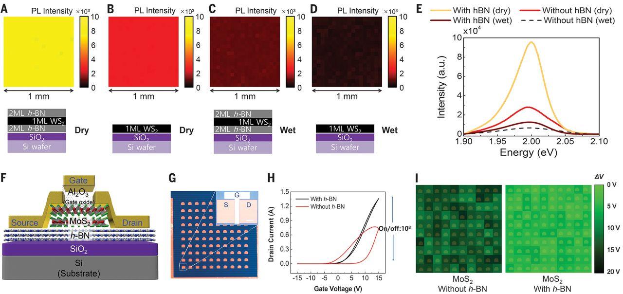
虽然可以用胶带剥离法形成微米尺度的二维(2D)异质结构薄片,但将二维薄片分离成单层却非常耗时,因为这是一个反复试验的过程。由于二维材料的成核障碍很高,因此通过直接生长来控制二维层的数量也很困难。我们展示了一种层分辨二维材料分割技术,通过分割在单个晶圆上生长的厚二维材料单堆,可以高通量生产晶圆级(直径 5 厘米)的多单层二维材料。六方氮化硼、二硫化钨、二硒化钨、二硫化钼和二硒化钼单层的晶圆级均匀性通过光致发光响应和电子导电性的实质性保留得到了验证。我们以单原子厚度分辨率制作了晶圆级范德华异质结构,包括场效应晶体管。本文章由计算机程序翻译,如有差异,请以英文原文为准。
Controlled crack propagation for atomic precision handling of wafer-scale two-dimensional materials
Although flakes of two-dimensional (2D) heterostructures at the micrometer scale can be formed with adhesive-tape exfoliation methods, isolation of 2D flakes into monolayers is extremely time consuming because it is a trial-and-error process. Controlling the number of 2D layers through direct growth also presents difficulty because of the high nucleation barrier on 2D materials. We demonstrate a layer-resolved 2D material splitting technique that permits high-throughput production of multiple monolayers of wafer-scale (5-centimeter diameter) 2D materials by splitting single stacks of thick 2D materials grown on a single wafer. Wafer-scale uniformity of hexagonal boron nitride, tungsten disulfide, tungsten diselenide, molybdenum disulfide, and molybdenum diselenide monolayers was verified by photoluminescence response and by substantial retention of electronic conductivity. We fabricated wafer-scale van der Waals heterostructures, including field-effect transistors, with single-atom thickness resolution.
求助全文
通过发布文献求助,成功后即可免费获取论文全文。
去求助
来源期刊
Science
综合性期刊-综合性期刊
CiteScore
61.10
自引率
0.90%
发文量
0
审稿时长
2.1 months
期刊介绍:
Science is a leading outlet for scientific news, commentary, and cutting-edge research. Through its print and online incarnations, Science reaches an estimated worldwide readership of more than one million. Science’s authorship is global too, and its articles consistently rank among the world's most cited research.
Science serves as a forum for discussion of important issues related to the advancement of science by publishing material on which a consensus has been reached as well as including the presentation of minority or conflicting points of view. Accordingly, all articles published in Science—including editorials, news and comment, and book reviews—are signed and reflect the individual views of the authors and not official points of view adopted by AAAS or the institutions with which the authors are affiliated.
Science seeks to publish those papers that are most influential in their fields or across fields and that will significantly advance scientific understanding. Selected papers should present novel and broadly important data, syntheses, or concepts. They should merit recognition by the wider scientific community and general public provided by publication in Science, beyond that provided by specialty journals. Science welcomes submissions from all fields of science and from any source. The editors are committed to the prompt evaluation and publication of submitted papers while upholding high standards that support reproducibility of published research. Science is published weekly; selected papers are published online ahead of print.
 求助内容:
求助内容: 应助结果提醒方式:


