在ITO上增强Zn-Ni合金纳米结构的非线性光学响应

IF 4.6 3区 工程技术 Q2 ENGINEERING, ELECTRICAL & ELECTRONIC
K.B. Manjunatha , Ramesh S. Bhat , S. Kshama Shetty , Dileep Ramakrishna , Yogesh Kalegowda , Poornesh P , Saikat Chattopadhyay , N. Selvakumar , Harish C. Barshilia
{"title":"在ITO上增强Zn-Ni合金纳米结构的非线性光学响应","authors":"K.B. Manjunatha ,&nbsp;Ramesh S. Bhat ,&nbsp;S. Kshama Shetty ,&nbsp;Dileep Ramakrishna ,&nbsp;Yogesh Kalegowda ,&nbsp;Poornesh P ,&nbsp;Saikat Chattopadhyay ,&nbsp;N. Selvakumar ,&nbsp;Harish C. Barshilia","doi":"10.1016/j.mssp.2025.110120","DOIUrl":null,"url":null,"abstract":"<div><div>This study reports the fabrication of Zn–Ni alloy nanostructures (ZN) on indium tin oxide (ITO) substrates via electrodeposition and investigates their nonlinear optical (NLO) and optical limiting behavior. Despite the promise of Zn-based nanostructures in NLO devices, their performance remains limited by weak field localization and inadequate surface engineering. This work addresses the knowledge gap by investigating how Ni alloying and surface oxidation in Zn–Ni nanostructures enhance local field effects and defect-mediated transitions, leading to improved nonlinear optical and optical limiting responses. Structural and spectroscopic analyses confirmed the γ-Zn–Ni alloy phase, ZnO/NiO surface oxides, and nanowall network morphologies. The nanostructures exhibited tunable band gaps between 2.95 and 3.17 eV, and high visible photoluminescence from defect states. The presence of surface oxidation suggests that the observed increase in local field effects may result from the high surface oxide density, as confirmed by Raman and photoluminescence data, and defect-mediated transitions, contributing to the observed strong optical nonlinearities. Specific NLO results include a two-photon absorption coefficient of ∼10<sup>−3</sup> cm/W under continuous-wave excitation and a three-photon absorption coefficient of ∼10<sup>−22</sup> m<sup>3</sup>/W<sup>2</sup> under nanosecond pulsed excitation, which are larger than/comparable to typical ZnO-based systems reported in literature. Optical limiting thresholds were also determined and compared with reported oxide nanostructures, demonstrating competitive or improved performance. These findings highlight the novelty of correlating alloy composition, nanowall morphology, and surface oxide density with enhanced third-order nonlinearities and efficient optical limiting, establishing Zn–Ni nanostructures as promising candidates for photonic and laser-protection devices.</div></div>","PeriodicalId":18240,"journal":{"name":"Materials Science in Semiconductor Processing","volume":"202 ","pages":"Article 110120"},"PeriodicalIF":4.6000,"publicationDate":"2025-10-14","publicationTypes":"Journal Article","fieldsOfStudy":null,"isOpenAccess":false,"openAccessPdf":"","citationCount":"0","resultStr":"{\"title\":\"Enhanced nonlinear optical response of Zn–Ni alloy nanostructures on ITO for optical limiting applications\",\"authors\":\"K.B. Manjunatha ,&nbsp;Ramesh S. Bhat ,&nbsp;S. Kshama Shetty ,&nbsp;Dileep Ramakrishna ,&nbsp;Yogesh Kalegowda ,&nbsp;Poornesh P ,&nbsp;Saikat Chattopadhyay ,&nbsp;N. Selvakumar ,&nbsp;Harish C. Barshilia\",\"doi\":\"10.1016/j.mssp.2025.110120\",\"DOIUrl\":null,\"url\":null,\"abstract\":\"<div><div>This study reports the fabrication of Zn–Ni alloy nanostructures (ZN) on indium tin oxide (ITO) substrates via electrodeposition and investigates their nonlinear optical (NLO) and optical limiting behavior. Despite the promise of Zn-based nanostructures in NLO devices, their performance remains limited by weak field localization and inadequate surface engineering. This work addresses the knowledge gap by investigating how Ni alloying and surface oxidation in Zn–Ni nanostructures enhance local field effects and defect-mediated transitions, leading to improved nonlinear optical and optical limiting responses. Structural and spectroscopic analyses confirmed the γ-Zn–Ni alloy phase, ZnO/NiO surface oxides, and nanowall network morphologies. The nanostructures exhibited tunable band gaps between 2.95 and 3.17 eV, and high visible photoluminescence from defect states. The presence of surface oxidation suggests that the observed increase in local field effects may result from the high surface oxide density, as confirmed by Raman and photoluminescence data, and defect-mediated transitions, contributing to the observed strong optical nonlinearities. Specific NLO results include a two-photon absorption coefficient of ∼10<sup>−3</sup> cm/W under continuous-wave excitation and a three-photon absorption coefficient of ∼10<sup>−22</sup> m<sup>3</sup>/W<sup>2</sup> under nanosecond pulsed excitation, which are larger than/comparable to typical ZnO-based systems reported in literature. Optical limiting thresholds were also determined and compared with reported oxide nanostructures, demonstrating competitive or improved performance. These findings highlight the novelty of correlating alloy composition, nanowall morphology, and surface oxide density with enhanced third-order nonlinearities and efficient optical limiting, establishing Zn–Ni nanostructures as promising candidates for photonic and laser-protection devices.</div></div>\",\"PeriodicalId\":18240,\"journal\":{\"name\":\"Materials Science in Semiconductor Processing\",\"volume\":\"202 \",\"pages\":\"Article 110120\"},\"PeriodicalIF\":4.6000,\"publicationDate\":\"2025-10-14\",\"publicationTypes\":\"Journal Article\",\"fieldsOfStudy\":null,\"isOpenAccess\":false,\"openAccessPdf\":\"\",\"citationCount\":\"0\",\"resultStr\":null,\"platform\":\"Semanticscholar\",\"paperid\":null,\"PeriodicalName\":\"Materials Science in Semiconductor Processing\",\"FirstCategoryId\":\"5\",\"ListUrlMain\":\"https://www.sciencedirect.com/science/article/pii/S1369800125008583\",\"RegionNum\":3,\"RegionCategory\":\"工程技术\",\"ArticlePicture\":[],\"TitleCN\":null,\"AbstractTextCN\":null,\"PMCID\":null,\"EPubDate\":\"\",\"PubModel\":\"\",\"JCR\":\"Q2\",\"JCRName\":\"ENGINEERING, ELECTRICAL & ELECTRONIC\",\"Score\":null,\"Total\":0}","platform":"Semanticscholar","paperid":null,"PeriodicalName":"Materials Science in Semiconductor Processing","FirstCategoryId":"5","ListUrlMain":"https://www.sciencedirect.com/science/article/pii/S1369800125008583","RegionNum":3,"RegionCategory":"工程技术","ArticlePicture":[],"TitleCN":null,"AbstractTextCN":null,"PMCID":null,"EPubDate":"","PubModel":"","JCR":"Q2","JCRName":"ENGINEERING, ELECTRICAL & ELECTRONIC","Score":null,"Total":0}
引用次数: 0

摘要

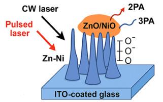
本研究报道了在氧化铟锡(ITO)衬底上电沉积制备ZN - ni合金纳米结构(ZN),并研究了其非线性光学(NLO)和光限行为。尽管锌基纳米结构在NLO器件中的应用前景广阔,但其性能仍然受到弱场局部化和表面工程不足的限制。本研究通过研究Zn-Ni纳米结构中的Ni合金化和表面氧化如何增强局部场效应和缺陷介导的转变,从而改善非线性光学和光极限响应,解决了这一知识缺口。结构和光谱分析证实了γ-Zn-Ni合金相、ZnO/NiO表面氧化物和纳米壁网络形态。该纳米结构具有2.95 ~ 3.17 eV的可调带隙,缺陷态具有较高的可见光致发光性能。表面氧化的存在表明,观察到的局部场效应的增加可能是由高表面氧化密度引起的,正如拉曼和光致发光数据所证实的那样,以及缺陷介导的跃迁,导致了观察到的强光学非线性。具体的NLO结果包括连续波激发下的双光子吸收系数为~ 10−3 cm/W,纳秒脉冲激发下的三光子吸收系数为~ 10−22 m3/W2,这些都大于或可与文献报道的典型zno基体系相媲美。光学极限阈值也被确定,并与已报道的氧化物纳米结构进行比较,显示出具有竞争力或改进的性能。这些发现强调了将合金成分、纳米壁形貌和表面氧化物密度与增强的三阶非线性和有效的光学限制联系起来的新新性,建立了锌-镍纳米结构作为光子和激光保护器件的有前途的候选者。
本文章由计算机程序翻译,如有差异,请以英文原文为准。

Enhanced nonlinear optical response of Zn–Ni alloy nanostructures on ITO for optical limiting applications

Enhanced nonlinear optical response of Zn–Ni alloy nanostructures on ITO for optical limiting applications
This study reports the fabrication of Zn–Ni alloy nanostructures (ZN) on indium tin oxide (ITO) substrates via electrodeposition and investigates their nonlinear optical (NLO) and optical limiting behavior. Despite the promise of Zn-based nanostructures in NLO devices, their performance remains limited by weak field localization and inadequate surface engineering. This work addresses the knowledge gap by investigating how Ni alloying and surface oxidation in Zn–Ni nanostructures enhance local field effects and defect-mediated transitions, leading to improved nonlinear optical and optical limiting responses. Structural and spectroscopic analyses confirmed the γ-Zn–Ni alloy phase, ZnO/NiO surface oxides, and nanowall network morphologies. The nanostructures exhibited tunable band gaps between 2.95 and 3.17 eV, and high visible photoluminescence from defect states. The presence of surface oxidation suggests that the observed increase in local field effects may result from the high surface oxide density, as confirmed by Raman and photoluminescence data, and defect-mediated transitions, contributing to the observed strong optical nonlinearities. Specific NLO results include a two-photon absorption coefficient of ∼10−3 cm/W under continuous-wave excitation and a three-photon absorption coefficient of ∼10−22 m3/W2 under nanosecond pulsed excitation, which are larger than/comparable to typical ZnO-based systems reported in literature. Optical limiting thresholds were also determined and compared with reported oxide nanostructures, demonstrating competitive or improved performance. These findings highlight the novelty of correlating alloy composition, nanowall morphology, and surface oxide density with enhanced third-order nonlinearities and efficient optical limiting, establishing Zn–Ni nanostructures as promising candidates for photonic and laser-protection devices.
求助全文
通过发布文献求助,成功后即可免费获取论文全文。 去求助
来源期刊
Materials Science in Semiconductor Processing
Materials Science in Semiconductor Processing 工程技术-材料科学:综合
CiteScore
8.00
自引率
4.90%
发文量
780
审稿时长
42 days
期刊介绍: Materials Science in Semiconductor Processing provides a unique forum for the discussion of novel processing, applications and theoretical studies of functional materials and devices for (opto)electronics, sensors, detectors, biotechnology and green energy. Each issue will aim to provide a snapshot of current insights, new achievements, breakthroughs and future trends in such diverse fields as microelectronics, energy conversion and storage, communications, biotechnology, (photo)catalysis, nano- and thin-film technology, hybrid and composite materials, chemical processing, vapor-phase deposition, device fabrication, and modelling, which are the backbone of advanced semiconductor processing and applications. Coverage will include: advanced lithography for submicron devices; etching and related topics; ion implantation; damage evolution and related issues; plasma and thermal CVD; rapid thermal processing; advanced metallization and interconnect schemes; thin dielectric layers, oxidation; sol-gel processing; chemical bath and (electro)chemical deposition; compound semiconductor processing; new non-oxide materials and their applications; (macro)molecular and hybrid materials; molecular dynamics, ab-initio methods, Monte Carlo, etc.; new materials and processes for discrete and integrated circuits; magnetic materials and spintronics; heterostructures and quantum devices; engineering of the electrical and optical properties of semiconductors; crystal growth mechanisms; reliability, defect density, intrinsic impurities and defects.
×
引用
GB/T 7714-2015
复制
MLA
复制
APA
复制
导出至
BibTeX EndNote RefMan NoteFirst NoteExpress
×
提示
您的信息不完整,为了账户安全,请先补充。
现在去补充
×
提示
您因"违规操作"
具体请查看互助需知
我知道了
×
提示
确定
请完成安全验证×
copy
已复制链接
快去分享给好友吧!
我知道了
右上角分享
点击右上角分享
0
联系我们:info@booksci.cn Book学术提供免费学术资源搜索服务,方便国内外学者检索中英文文献。致力于提供最便捷和优质的服务体验。 Copyright © 2023 布克学术 All rights reserved.
京ICP备2023020795号-1
ghs 京公网安备 11010802042870号
Book学术文献互助
Book学术文献互助群
群 号:604180095
Book学术官方微信