具有SiGeSn势垒的GeSn量子阱的高迁移率和静电特性

IF 5.3 2区 材料科学 Q2 MATERIALS SCIENCE, MULTIDISCIPLINARY
Christopher R. Allemang, David Lidsky, Peter Sharma, Shang Liu, Jifeng Liu, Yunsheng Qiu, Shuiqing Yu, Tzu-Ming Lu
{"title":"具有SiGeSn势垒的GeSn量子阱的高迁移率和静电特性","authors":"Christopher R. Allemang, David Lidsky, Peter Sharma, Shang Liu, Jifeng Liu, Yunsheng Qiu, Shuiqing Yu, Tzu-Ming Lu","doi":"10.1002/aelm.202500460","DOIUrl":null,"url":null,"abstract":"GeSn is an emerging material with potential applications in next-generation integrated optoelectronics and quantum information processing. While GeSn/SiGeSn quantum wells exhibit promising optical properties, their electrical transport characteristics and governing electrostatics in gated structures remain unexplored. Heterostructure field-effect transistors are fabricated using GeSn/SiGeSn quantum wells and electronic transport properties of 2D holes are characterized. At 2 K, heterostructure field-effect transistors with well/barrier compositions of Ge<sub>0.945</sub>Sn<sub>0.055</sub>/Si<sub>0.03</sub>Ge<sub>0.93</sub>Sn<sub>0.04</sub> and Ge<sub>0.9</sub>Sn<sub>0.1</sub>/Si<sub>0.017</sub>Ge<sub>0.927</sub>Sn<sub>0.056</sub>, show peak mobilities of 9000 and 19 000 cm<sup>2</sup>/Vs, respectively, the latter setting a record for the highest mobility reported for GeSn quantum wells with a Sn concentration around 6 % or greater. Remarkably, at low carrier densities, devices with a SiGeSn barrier exhibit mobilities several times higher than previously reported for GeSn quantum wells with a Ge barrier. This higher mobility contrasts with the expectation that alloy scattering from the barrier would reduce carrier mobility. Two mechanisms based on atom probe tomography data analyses are proposed: i) unintentionally improved SiGeSn/GeSn interface and/or ii) reduced alloy scattering from short-range order. Significant current–voltage hysteresis is observed, with the effective threshold gate voltage shifting by more than 5 V, attributed to non-equilibrium trapped charge at various interfaces within the SiGeSn heterostructure.","PeriodicalId":110,"journal":{"name":"Advanced Electronic Materials","volume":"109 1","pages":""},"PeriodicalIF":5.3000,"publicationDate":"2025-10-09","publicationTypes":"Journal Article","fieldsOfStudy":null,"isOpenAccess":false,"openAccessPdf":"","citationCount":"0","resultStr":"{\"title\":\"High Mobility and Electrostatics in GeSn Quantum Wells With SiGeSn Barriers\",\"authors\":\"Christopher R. Allemang, David Lidsky, Peter Sharma, Shang Liu, Jifeng Liu, Yunsheng Qiu, Shuiqing Yu, Tzu-Ming Lu\",\"doi\":\"10.1002/aelm.202500460\",\"DOIUrl\":null,\"url\":null,\"abstract\":\"GeSn is an emerging material with potential applications in next-generation integrated optoelectronics and quantum information processing. While GeSn/SiGeSn quantum wells exhibit promising optical properties, their electrical transport characteristics and governing electrostatics in gated structures remain unexplored. Heterostructure field-effect transistors are fabricated using GeSn/SiGeSn quantum wells and electronic transport properties of 2D holes are characterized. At 2 K, heterostructure field-effect transistors with well/barrier compositions of Ge<sub>0.945</sub>Sn<sub>0.055</sub>/Si<sub>0.03</sub>Ge<sub>0.93</sub>Sn<sub>0.04</sub> and Ge<sub>0.9</sub>Sn<sub>0.1</sub>/Si<sub>0.017</sub>Ge<sub>0.927</sub>Sn<sub>0.056</sub>, show peak mobilities of 9000 and 19 000 cm<sup>2</sup>/Vs, respectively, the latter setting a record for the highest mobility reported for GeSn quantum wells with a Sn concentration around 6 % or greater. Remarkably, at low carrier densities, devices with a SiGeSn barrier exhibit mobilities several times higher than previously reported for GeSn quantum wells with a Ge barrier. This higher mobility contrasts with the expectation that alloy scattering from the barrier would reduce carrier mobility. Two mechanisms based on atom probe tomography data analyses are proposed: i) unintentionally improved SiGeSn/GeSn interface and/or ii) reduced alloy scattering from short-range order. Significant current–voltage hysteresis is observed, with the effective threshold gate voltage shifting by more than 5 V, attributed to non-equilibrium trapped charge at various interfaces within the SiGeSn heterostructure.\",\"PeriodicalId\":110,\"journal\":{\"name\":\"Advanced Electronic Materials\",\"volume\":\"109 1\",\"pages\":\"\"},\"PeriodicalIF\":5.3000,\"publicationDate\":\"2025-10-09\",\"publicationTypes\":\"Journal Article\",\"fieldsOfStudy\":null,\"isOpenAccess\":false,\"openAccessPdf\":\"\",\"citationCount\":\"0\",\"resultStr\":null,\"platform\":\"Semanticscholar\",\"paperid\":null,\"PeriodicalName\":\"Advanced Electronic Materials\",\"FirstCategoryId\":\"88\",\"ListUrlMain\":\"https://doi.org/10.1002/aelm.202500460\",\"RegionNum\":2,\"RegionCategory\":\"材料科学\",\"ArticlePicture\":[],\"TitleCN\":null,\"AbstractTextCN\":null,\"PMCID\":null,\"EPubDate\":\"\",\"PubModel\":\"\",\"JCR\":\"Q2\",\"JCRName\":\"MATERIALS SCIENCE, MULTIDISCIPLINARY\",\"Score\":null,\"Total\":0}","platform":"Semanticscholar","paperid":null,"PeriodicalName":"Advanced Electronic Materials","FirstCategoryId":"88","ListUrlMain":"https://doi.org/10.1002/aelm.202500460","RegionNum":2,"RegionCategory":"材料科学","ArticlePicture":[],"TitleCN":null,"AbstractTextCN":null,"PMCID":null,"EPubDate":"","PubModel":"","JCR":"Q2","JCRName":"MATERIALS SCIENCE, MULTIDISCIPLINARY","Score":null,"Total":0}
引用次数: 0

摘要

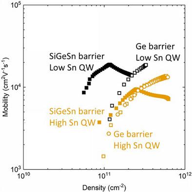
GeSn是一种新兴材料,在下一代集成光电子和量子信息处理中具有潜在的应用前景。虽然GeSn/SiGeSn量子阱表现出很好的光学特性,但它们的电输运特性和门控结构中的控制静电仍未被探索。利用GeSn/SiGeSn量子阱制备了异质结构场效应晶体管,并对二维空穴的电子输运特性进行了表征。在2k时,阱势垒组成为Ge0.945Sn0.055/Si0.03Ge0.93Sn0.04和Ge0.9Sn0.1/Si0.017Ge0.927Sn0.056的异质结构场效应晶体管的迁移率峰值分别为9000和19000 cm2/Vs,后者创下了Sn浓度在6%左右或更高时GeSn量子阱的最高迁移率记录。值得注意的是,在低载流子密度下,具有SiGeSn势垒的器件的迁移率比先前报道的具有Ge势垒的GeSn量子阱高几倍。这种高迁移率与合金从势垒散射会降低载流子迁移率的预期形成对比。基于原子探针层析成像数据分析提出了两种机制:i)无意中改善了SiGeSn/GeSn界面和/或ii)减少了合金的短程散射。由于SiGeSn异质结构中各界面处的非平衡捕获电荷,观察到明显的电流-电压滞后,有效阈值门电压移动超过5 V。
本文章由计算机程序翻译,如有差异,请以英文原文为准。

High Mobility and Electrostatics in GeSn Quantum Wells With SiGeSn Barriers

High Mobility and Electrostatics in GeSn Quantum Wells With SiGeSn Barriers
GeSn is an emerging material with potential applications in next-generation integrated optoelectronics and quantum information processing. While GeSn/SiGeSn quantum wells exhibit promising optical properties, their electrical transport characteristics and governing electrostatics in gated structures remain unexplored. Heterostructure field-effect transistors are fabricated using GeSn/SiGeSn quantum wells and electronic transport properties of 2D holes are characterized. At 2 K, heterostructure field-effect transistors with well/barrier compositions of Ge0.945Sn0.055/Si0.03Ge0.93Sn0.04 and Ge0.9Sn0.1/Si0.017Ge0.927Sn0.056, show peak mobilities of 9000 and 19 000 cm2/Vs, respectively, the latter setting a record for the highest mobility reported for GeSn quantum wells with a Sn concentration around 6 % or greater. Remarkably, at low carrier densities, devices with a SiGeSn barrier exhibit mobilities several times higher than previously reported for GeSn quantum wells with a Ge barrier. This higher mobility contrasts with the expectation that alloy scattering from the barrier would reduce carrier mobility. Two mechanisms based on atom probe tomography data analyses are proposed: i) unintentionally improved SiGeSn/GeSn interface and/or ii) reduced alloy scattering from short-range order. Significant current–voltage hysteresis is observed, with the effective threshold gate voltage shifting by more than 5 V, attributed to non-equilibrium trapped charge at various interfaces within the SiGeSn heterostructure.
求助全文
通过发布文献求助,成功后即可免费获取论文全文。 去求助
来源期刊
Advanced Electronic Materials
Advanced Electronic Materials NANOSCIENCE & NANOTECHNOLOGYMATERIALS SCIE-MATERIALS SCIENCE, MULTIDISCIPLINARY
CiteScore
11.00
自引率
3.20%
发文量
433
期刊介绍: Advanced Electronic Materials is an interdisciplinary forum for peer-reviewed, high-quality, high-impact research in the fields of materials science, physics, and engineering of electronic and magnetic materials. It includes research on physics and physical properties of electronic and magnetic materials, spintronics, electronics, device physics and engineering, micro- and nano-electromechanical systems, and organic electronics, in addition to fundamental research.
×
引用
GB/T 7714-2015
复制
MLA
复制
APA
复制
导出至
BibTeX EndNote RefMan NoteFirst NoteExpress
×
提示
您的信息不完整,为了账户安全,请先补充。
现在去补充
×
提示
您因"违规操作"
具体请查看互助需知
我知道了
×
提示
确定
请完成安全验证×
copy
已复制链接
快去分享给好友吧!
我知道了
右上角分享
点击右上角分享
0
联系我们:info@booksci.cn Book学术提供免费学术资源搜索服务,方便国内外学者检索中英文文献。致力于提供最便捷和优质的服务体验。 Copyright © 2023 布克学术 All rights reserved.
京ICP备2023020795号-1
ghs 京公网安备 11010802042870号
Book学术文献互助
Book学术文献互助群
群 号:604180095
Book学术官方微信