Al2O3/TiO2纳米层沉积原子层的组成控制和电性能

IF 4.6 3区 工程技术 Q2 ENGINEERING, ELECTRICAL & ELECTRONIC
Yuan Xu , Ying Pan , Lingshan Gao , Faqiang Zhang , Mingsheng Ma , Jie Liang , Zhifu Liu
{"title":"Al2O3/TiO2纳米层沉积原子层的组成控制和电性能","authors":"Yuan Xu ,&nbsp;Ying Pan ,&nbsp;Lingshan Gao ,&nbsp;Faqiang Zhang ,&nbsp;Mingsheng Ma ,&nbsp;Jie Liang ,&nbsp;Zhifu Liu","doi":"10.1016/j.mssp.2025.110105","DOIUrl":null,"url":null,"abstract":"<div><div>Nanolaminate Al<sub>2</sub>O<sub>3</sub>/TiO<sub>2</sub> (ATO) dielectric films were fabricated using atomic layer deposition (ALD) and evaluated as insulating layers in metal-oxide-semiconductor (MOS) capacitors. The TiO<sub>2</sub> content within the nanolaminates was systematically varied to modulating both optical and electrical properties. Precise thickness control and stable growth per cycle (GPC) for each sublayer were achieved at a deposition temperature of 200 °C. Spectroscopic ellipsometry revealed that increasing TiO<sub>2</sub> content led to a higher refractive index and optical dielectric constant, accompanied by a reduction in bandgap (E<sub>g</sub>). Microstructural analysis demonstrated that the laminated structure suppressed surface roughness and enhanced interfacial quality. Electrical measurements showed that increasing the TiO<sub>2</sub> fraction enhanced the accumulation capacitance due to its high dielectric constant, but also resulted in higher leakage current, attributed to trap-assisted and Poole-Frenkel (P-F) conduction mechanisms. Notably, the introduction of Al<sub>2</sub>O<sub>3</sub> sublayers as insulating barriers effectively suppressed leakage pathways and stabilized charge transport. These findings suggest that the ATO nanolaminate structure is a promising candidate for high-k gate dielectrics in advanced semiconductor applications.</div></div>","PeriodicalId":18240,"journal":{"name":"Materials Science in Semiconductor Processing","volume":"201 ","pages":"Article 110105"},"PeriodicalIF":4.6000,"publicationDate":"2025-10-01","publicationTypes":"Journal Article","fieldsOfStudy":null,"isOpenAccess":false,"openAccessPdf":"","citationCount":"0","resultStr":"{\"title\":\"Compositional control and electrical performance of atomic layer deposited Al2O3/TiO2 nanolaminates\",\"authors\":\"Yuan Xu ,&nbsp;Ying Pan ,&nbsp;Lingshan Gao ,&nbsp;Faqiang Zhang ,&nbsp;Mingsheng Ma ,&nbsp;Jie Liang ,&nbsp;Zhifu Liu\",\"doi\":\"10.1016/j.mssp.2025.110105\",\"DOIUrl\":null,\"url\":null,\"abstract\":\"<div><div>Nanolaminate Al<sub>2</sub>O<sub>3</sub>/TiO<sub>2</sub> (ATO) dielectric films were fabricated using atomic layer deposition (ALD) and evaluated as insulating layers in metal-oxide-semiconductor (MOS) capacitors. The TiO<sub>2</sub> content within the nanolaminates was systematically varied to modulating both optical and electrical properties. Precise thickness control and stable growth per cycle (GPC) for each sublayer were achieved at a deposition temperature of 200 °C. Spectroscopic ellipsometry revealed that increasing TiO<sub>2</sub> content led to a higher refractive index and optical dielectric constant, accompanied by a reduction in bandgap (E<sub>g</sub>). Microstructural analysis demonstrated that the laminated structure suppressed surface roughness and enhanced interfacial quality. Electrical measurements showed that increasing the TiO<sub>2</sub> fraction enhanced the accumulation capacitance due to its high dielectric constant, but also resulted in higher leakage current, attributed to trap-assisted and Poole-Frenkel (P-F) conduction mechanisms. Notably, the introduction of Al<sub>2</sub>O<sub>3</sub> sublayers as insulating barriers effectively suppressed leakage pathways and stabilized charge transport. These findings suggest that the ATO nanolaminate structure is a promising candidate for high-k gate dielectrics in advanced semiconductor applications.</div></div>\",\"PeriodicalId\":18240,\"journal\":{\"name\":\"Materials Science in Semiconductor Processing\",\"volume\":\"201 \",\"pages\":\"Article 110105\"},\"PeriodicalIF\":4.6000,\"publicationDate\":\"2025-10-01\",\"publicationTypes\":\"Journal Article\",\"fieldsOfStudy\":null,\"isOpenAccess\":false,\"openAccessPdf\":\"\",\"citationCount\":\"0\",\"resultStr\":null,\"platform\":\"Semanticscholar\",\"paperid\":null,\"PeriodicalName\":\"Materials Science in Semiconductor Processing\",\"FirstCategoryId\":\"5\",\"ListUrlMain\":\"https://www.sciencedirect.com/science/article/pii/S1369800125008431\",\"RegionNum\":3,\"RegionCategory\":\"工程技术\",\"ArticlePicture\":[],\"TitleCN\":null,\"AbstractTextCN\":null,\"PMCID\":null,\"EPubDate\":\"\",\"PubModel\":\"\",\"JCR\":\"Q2\",\"JCRName\":\"ENGINEERING, ELECTRICAL & ELECTRONIC\",\"Score\":null,\"Total\":0}","platform":"Semanticscholar","paperid":null,"PeriodicalName":"Materials Science in Semiconductor Processing","FirstCategoryId":"5","ListUrlMain":"https://www.sciencedirect.com/science/article/pii/S1369800125008431","RegionNum":3,"RegionCategory":"工程技术","ArticlePicture":[],"TitleCN":null,"AbstractTextCN":null,"PMCID":null,"EPubDate":"","PubModel":"","JCR":"Q2","JCRName":"ENGINEERING, ELECTRICAL & ELECTRONIC","Score":null,"Total":0}
引用次数: 0

摘要

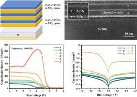
采用原子层沉积(ALD)法制备了纳米层Al2O3/TiO2 (ATO)介电膜,并对其作为金属氧化物半导体(MOS)电容器的绝缘层进行了评价。纳米层合物中的TiO2含量被系统地改变以调制光学和电学性质。在200°C的沉积温度下,实现了每个子层的精确厚度控制和稳定的每周期生长(GPC)。椭偏光谱分析表明,TiO2含量的增加导致材料的折射率和介电常数增加,同时带隙减小(Eg)。显微组织分析表明,层合结构抑制了表面粗糙度,提高了界面质量。电学测量表明,TiO2分数的增加由于其高介电常数而增强了积累电容,但由于陷阱辅助和Poole-Frenkel (P-F)传导机制,也导致了更高的泄漏电流。值得注意的是,Al2O3亚层作为绝缘屏障的引入有效地抑制了泄漏通路并稳定了电荷输运。这些发现表明,ATO纳米层合结构是先进半导体应用中高k栅极电介质的有希望的候选者。
本文章由计算机程序翻译,如有差异,请以英文原文为准。

Compositional control and electrical performance of atomic layer deposited Al2O3/TiO2 nanolaminates

Compositional control and electrical performance of atomic layer deposited Al2O3/TiO2 nanolaminates
Nanolaminate Al2O3/TiO2 (ATO) dielectric films were fabricated using atomic layer deposition (ALD) and evaluated as insulating layers in metal-oxide-semiconductor (MOS) capacitors. The TiO2 content within the nanolaminates was systematically varied to modulating both optical and electrical properties. Precise thickness control and stable growth per cycle (GPC) for each sublayer were achieved at a deposition temperature of 200 °C. Spectroscopic ellipsometry revealed that increasing TiO2 content led to a higher refractive index and optical dielectric constant, accompanied by a reduction in bandgap (Eg). Microstructural analysis demonstrated that the laminated structure suppressed surface roughness and enhanced interfacial quality. Electrical measurements showed that increasing the TiO2 fraction enhanced the accumulation capacitance due to its high dielectric constant, but also resulted in higher leakage current, attributed to trap-assisted and Poole-Frenkel (P-F) conduction mechanisms. Notably, the introduction of Al2O3 sublayers as insulating barriers effectively suppressed leakage pathways and stabilized charge transport. These findings suggest that the ATO nanolaminate structure is a promising candidate for high-k gate dielectrics in advanced semiconductor applications.
求助全文
通过发布文献求助,成功后即可免费获取论文全文。 去求助
来源期刊
Materials Science in Semiconductor Processing
Materials Science in Semiconductor Processing 工程技术-材料科学:综合
CiteScore
8.00
自引率
4.90%
发文量
780
审稿时长
42 days
期刊介绍: Materials Science in Semiconductor Processing provides a unique forum for the discussion of novel processing, applications and theoretical studies of functional materials and devices for (opto)electronics, sensors, detectors, biotechnology and green energy. Each issue will aim to provide a snapshot of current insights, new achievements, breakthroughs and future trends in such diverse fields as microelectronics, energy conversion and storage, communications, biotechnology, (photo)catalysis, nano- and thin-film technology, hybrid and composite materials, chemical processing, vapor-phase deposition, device fabrication, and modelling, which are the backbone of advanced semiconductor processing and applications. Coverage will include: advanced lithography for submicron devices; etching and related topics; ion implantation; damage evolution and related issues; plasma and thermal CVD; rapid thermal processing; advanced metallization and interconnect schemes; thin dielectric layers, oxidation; sol-gel processing; chemical bath and (electro)chemical deposition; compound semiconductor processing; new non-oxide materials and their applications; (macro)molecular and hybrid materials; molecular dynamics, ab-initio methods, Monte Carlo, etc.; new materials and processes for discrete and integrated circuits; magnetic materials and spintronics; heterostructures and quantum devices; engineering of the electrical and optical properties of semiconductors; crystal growth mechanisms; reliability, defect density, intrinsic impurities and defects.
×
引用
GB/T 7714-2015
复制
MLA
复制
APA
复制
导出至
BibTeX EndNote RefMan NoteFirst NoteExpress
×
提示
您的信息不完整,为了账户安全,请先补充。
现在去补充
×
提示
您因"违规操作"
具体请查看互助需知
我知道了
×
提示
确定
请完成安全验证×
copy
已复制链接
快去分享给好友吧!
我知道了
右上角分享
点击右上角分享
0
联系我们:info@booksci.cn Book学术提供免费学术资源搜索服务,方便国内外学者检索中英文文献。致力于提供最便捷和优质的服务体验。 Copyright © 2023 布克学术 All rights reserved.
京ICP备2023020795号-1
ghs 京公网安备 11010802042870号
Book学术文献互助
Book学术文献互助群
群 号:604180095
Book学术官方微信