迈向埋藏在钻石中的全碳电子器件
IF 5.3
2区 材料科学
Q2 MATERIALS SCIENCE, MULTIDISCIPLINARY
引用次数: 0
摘要
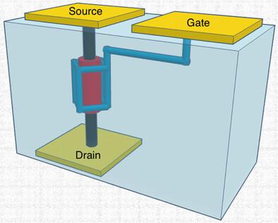
这项工作研究了利用飞秒激光加工在金刚石衬底内制造具有不同电学行为的各种纳米碳结构。实现金刚石掺杂的传统方法有明显的缺点,包括具有挑战性的生长曲线、有限的环境稳定性和次优的拟垂直结构。在这里,研究人员证明了激光写入纳米碳网络(ncn)直接缓解了这些问题,展示了埋藏在金刚石中的坚固而精确的电气结构的高度可重复制造,并且在重复的温度和电压循环中证明了稳定性。通过改变激光脉冲重复率(PRR),改性金刚石实现了从欧姆导电到半导体/双极性行为的转变。此外,一个概念验证,全碳晶体管架构埋在大块钻石,展示了使用激光写入工艺集成器件制造的潜力。本文章由计算机程序翻译,如有差异,请以英文原文为准。
Toward All-Carbon Electronics Buried in Diamond
This work investigates the use of femtosecond laser processing to fabricate various nanocarbon structures with distinct electrical behaviors within diamond substrates. Conventional approaches for achieving diamond doping have significant disadvantages, including challenging growth profiles, limited environmental stability, and sub-optimal psuedo-vertical structures. Here, it is demonstrated that laser-written nanocarbon networks (NCNs) directly alleviate these issues, demonstrating the highly repeatable fabrication of robust and precise electrical architectures buried in diamond with proven stability over repeated temperature and voltage cycling. By varying the laser pulse repetition rate (PRR), a transition from Ohmic conductive to semiconductive/ambipolar behavior is achieved in the modified diamond. Furthermore, a proof-of-concept, all-carbon transistor architecture buried within the bulk diamond is presented, showcasing the potential for integrated device fabrication using the laser-writing process.
求助全文
通过发布文献求助,成功后即可免费获取论文全文。
去求助
来源期刊

Advanced Electronic Materials
NANOSCIENCE & NANOTECHNOLOGYMATERIALS SCIE-MATERIALS SCIENCE, MULTIDISCIPLINARY
CiteScore
11.00
自引率
3.20%
发文量
433
期刊介绍:
Advanced Electronic Materials is an interdisciplinary forum for peer-reviewed, high-quality, high-impact research in the fields of materials science, physics, and engineering of electronic and magnetic materials. It includes research on physics and physical properties of electronic and magnetic materials, spintronics, electronics, device physics and engineering, micro- and nano-electromechanical systems, and organic electronics, in addition to fundamental research.
 求助内容:
求助内容: 应助结果提醒方式:


