Fan Yang, Haizeng Song, Shunshun Yang, Yichun Cui, Shafqat Hussain, Xueqian Sun, Youwen Liu, Yi Shi and Linglong Zhang
{"title":"高温光通信中二维范德华异质结构的界面工程","authors":"Fan Yang, Haizeng Song, Shunshun Yang, Yichun Cui, Shafqat Hussain, Xueqian Sun, Youwen Liu, Yi Shi and Linglong Zhang","doi":"10.1039/D5TC02092A","DOIUrl":null,"url":null,"abstract":"<p >Two-dimensional (2D) semiconductor materials maintain high carrier mobility, exceptional physical properties, thermal stability, and highly tunable band structures, making them ideal for designing high-temperature field-effect transistors (FETs) and photodiodes. However, most atoms of these materials are located on the surface, making them susceptible to degradation due to oxidation and decomposition at high temperatures. Here, we employed hexagonal boron nitride (hBN) to encapsulate molybdenum disulfide (MoS<small><sub>2</sub></small>), resulting in enhanced operation stability at temperatures above 523 K. Temperature-dependent photoluminescence (PL) measurements reveal that hBN encapsulation increases the activation energy (<em>E</em><small><sub>a</sub></small> ∼ 67 meV), indicating superior thermal stability. Additionally, the hBN-encapsulated tungsten diselenide (WSe<small><sub>2</sub></small>)–MoS<small><sub>2</sub></small> p–n junction exhibits a thermally stable ideality factor of ∼1.149 at 558 K. By leveraging the stable photoresponse at high temperatures, we further successfully realized a light communication system with enhanced security and reliability. These findings can pave the way for the development of 2D FETs and photodiodes in extreme environments.</p>","PeriodicalId":84,"journal":{"name":"Journal of Materials Chemistry C","volume":" 37","pages":" 19308-19315"},"PeriodicalIF":5.1000,"publicationDate":"2025-08-11","publicationTypes":"Journal Article","fieldsOfStudy":null,"isOpenAccess":false,"openAccessPdf":"","citationCount":"0","resultStr":"{\"title\":\"Interface engineering of 2D van der Waals heterostructures for high-temperature optical communication\",\"authors\":\"Fan Yang, Haizeng Song, Shunshun Yang, Yichun Cui, Shafqat Hussain, Xueqian Sun, Youwen Liu, Yi Shi and Linglong Zhang\",\"doi\":\"10.1039/D5TC02092A\",\"DOIUrl\":null,\"url\":null,\"abstract\":\"<p >Two-dimensional (2D) semiconductor materials maintain high carrier mobility, exceptional physical properties, thermal stability, and highly tunable band structures, making them ideal for designing high-temperature field-effect transistors (FETs) and photodiodes. However, most atoms of these materials are located on the surface, making them susceptible to degradation due to oxidation and decomposition at high temperatures. Here, we employed hexagonal boron nitride (hBN) to encapsulate molybdenum disulfide (MoS<small><sub>2</sub></small>), resulting in enhanced operation stability at temperatures above 523 K. Temperature-dependent photoluminescence (PL) measurements reveal that hBN encapsulation increases the activation energy (<em>E</em><small><sub>a</sub></small> ∼ 67 meV), indicating superior thermal stability. Additionally, the hBN-encapsulated tungsten diselenide (WSe<small><sub>2</sub></small>)–MoS<small><sub>2</sub></small> p–n junction exhibits a thermally stable ideality factor of ∼1.149 at 558 K. By leveraging the stable photoresponse at high temperatures, we further successfully realized a light communication system with enhanced security and reliability. These findings can pave the way for the development of 2D FETs and photodiodes in extreme environments.</p>\",\"PeriodicalId\":84,\"journal\":{\"name\":\"Journal of Materials Chemistry C\",\"volume\":\" 37\",\"pages\":\" 19308-19315\"},\"PeriodicalIF\":5.1000,\"publicationDate\":\"2025-08-11\",\"publicationTypes\":\"Journal Article\",\"fieldsOfStudy\":null,\"isOpenAccess\":false,\"openAccessPdf\":\"\",\"citationCount\":\"0\",\"resultStr\":null,\"platform\":\"Semanticscholar\",\"paperid\":null,\"PeriodicalName\":\"Journal of Materials Chemistry C\",\"FirstCategoryId\":\"1\",\"ListUrlMain\":\"https://pubs.rsc.org/en/content/articlelanding/2025/tc/d5tc02092a\",\"RegionNum\":2,\"RegionCategory\":\"材料科学\",\"ArticlePicture\":[],\"TitleCN\":null,\"AbstractTextCN\":null,\"PMCID\":null,\"EPubDate\":\"\",\"PubModel\":\"\",\"JCR\":\"Q2\",\"JCRName\":\"MATERIALS SCIENCE, MULTIDISCIPLINARY\",\"Score\":null,\"Total\":0}","platform":"Semanticscholar","paperid":null,"PeriodicalName":"Journal of Materials Chemistry C","FirstCategoryId":"1","ListUrlMain":"https://pubs.rsc.org/en/content/articlelanding/2025/tc/d5tc02092a","RegionNum":2,"RegionCategory":"材料科学","ArticlePicture":[],"TitleCN":null,"AbstractTextCN":null,"PMCID":null,"EPubDate":"","PubModel":"","JCR":"Q2","JCRName":"MATERIALS SCIENCE, MULTIDISCIPLINARY","Score":null,"Total":0}
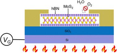
Interface engineering of 2D van der Waals heterostructures for high-temperature optical communication
Two-dimensional (2D) semiconductor materials maintain high carrier mobility, exceptional physical properties, thermal stability, and highly tunable band structures, making them ideal for designing high-temperature field-effect transistors (FETs) and photodiodes. However, most atoms of these materials are located on the surface, making them susceptible to degradation due to oxidation and decomposition at high temperatures. Here, we employed hexagonal boron nitride (hBN) to encapsulate molybdenum disulfide (MoS2), resulting in enhanced operation stability at temperatures above 523 K. Temperature-dependent photoluminescence (PL) measurements reveal that hBN encapsulation increases the activation energy (Ea ∼ 67 meV), indicating superior thermal stability. Additionally, the hBN-encapsulated tungsten diselenide (WSe2)–MoS2 p–n junction exhibits a thermally stable ideality factor of ∼1.149 at 558 K. By leveraging the stable photoresponse at high temperatures, we further successfully realized a light communication system with enhanced security and reliability. These findings can pave the way for the development of 2D FETs and photodiodes in extreme environments.
期刊介绍:
The Journal of Materials Chemistry is divided into three distinct sections, A, B, and C, each catering to specific applications of the materials under study:
Journal of Materials Chemistry A focuses primarily on materials intended for applications in energy and sustainability.
Journal of Materials Chemistry B specializes in materials designed for applications in biology and medicine.
Journal of Materials Chemistry C is dedicated to materials suitable for applications in optical, magnetic, and electronic devices.
Example topic areas within the scope of Journal of Materials Chemistry C are listed below. This list is neither exhaustive nor exclusive.
Bioelectronics
Conductors
Detectors
Dielectrics
Displays
Ferroelectrics
Lasers
LEDs
Lighting
Liquid crystals
Memory
Metamaterials
Multiferroics
Photonics
Photovoltaics
Semiconductors
Sensors
Single molecule conductors
Spintronics
Superconductors
Thermoelectrics
Topological insulators
Transistors

 求助内容:
求助内容: 应助结果提醒方式:


