{"title":"利用电光刻技术制造无电阻光掩膜","authors":"S.N. Ghosh, S. Talukder","doi":"10.1016/j.mne.2025.100320","DOIUrl":null,"url":null,"abstract":"<div><div>Photolithography is the most widely used lithography technique for commercial fabrication of micro-devices as well as for research and development purposes. However, to perform photolithography, we need a photomask containing the desired pattern. Conventional methods of photomask fabrication involve either photolithography using a direct laser writer or electron-beam lithography. Interestingly, the rise of sequential write scanning probe lithography (SPL) techniques has given rise to various novel methods of direct photomask writing. In this study, we focus on photomask fabrication using a SPL technique, known as ‘Electrolithography’ (ELG), with which multi-scale features can be easily patterned. This is a subtractive lithography technique that involves direct patterning on chromium (Cr) thin films. Being an electrical and direct-write process, ELG bypasses the need for high-power UV laser, electron gun, and polymer resist layers thereby making the process cost-effective and carbon-efficient. We propose a resistless, reliable and novel photomask fabrication process, using the ELG technique, based on a bimetallic architecture. Using the proposed method, we were able to obtain lines having a width of <2 μm, in the best case, and lines with a width < 10 μm repeatedly. We were also able to transfer the fabricated patterns reliably and repeatedly onto a material of choice.</div></div>","PeriodicalId":37111,"journal":{"name":"Micro and Nano Engineering","volume":"29 ","pages":"Article 100320"},"PeriodicalIF":3.1000,"publicationDate":"2025-09-12","publicationTypes":"Journal Article","fieldsOfStudy":null,"isOpenAccess":false,"openAccessPdf":"","citationCount":"0","resultStr":"{\"title\":\"Resistless photomask fabrication using electrolithography\",\"authors\":\"S.N. Ghosh, S. Talukder\",\"doi\":\"10.1016/j.mne.2025.100320\",\"DOIUrl\":null,\"url\":null,\"abstract\":\"<div><div>Photolithography is the most widely used lithography technique for commercial fabrication of micro-devices as well as for research and development purposes. However, to perform photolithography, we need a photomask containing the desired pattern. Conventional methods of photomask fabrication involve either photolithography using a direct laser writer or electron-beam lithography. Interestingly, the rise of sequential write scanning probe lithography (SPL) techniques has given rise to various novel methods of direct photomask writing. In this study, we focus on photomask fabrication using a SPL technique, known as ‘Electrolithography’ (ELG), with which multi-scale features can be easily patterned. This is a subtractive lithography technique that involves direct patterning on chromium (Cr) thin films. Being an electrical and direct-write process, ELG bypasses the need for high-power UV laser, electron gun, and polymer resist layers thereby making the process cost-effective and carbon-efficient. We propose a resistless, reliable and novel photomask fabrication process, using the ELG technique, based on a bimetallic architecture. Using the proposed method, we were able to obtain lines having a width of <2 μm, in the best case, and lines with a width < 10 μm repeatedly. We were also able to transfer the fabricated patterns reliably and repeatedly onto a material of choice.</div></div>\",\"PeriodicalId\":37111,\"journal\":{\"name\":\"Micro and Nano Engineering\",\"volume\":\"29 \",\"pages\":\"Article 100320\"},\"PeriodicalIF\":3.1000,\"publicationDate\":\"2025-09-12\",\"publicationTypes\":\"Journal Article\",\"fieldsOfStudy\":null,\"isOpenAccess\":false,\"openAccessPdf\":\"\",\"citationCount\":\"0\",\"resultStr\":null,\"platform\":\"Semanticscholar\",\"paperid\":null,\"PeriodicalName\":\"Micro and Nano Engineering\",\"FirstCategoryId\":\"1085\",\"ListUrlMain\":\"https://www.sciencedirect.com/science/article/pii/S2590007225000267\",\"RegionNum\":0,\"RegionCategory\":null,\"ArticlePicture\":[],\"TitleCN\":null,\"AbstractTextCN\":null,\"PMCID\":null,\"EPubDate\":\"\",\"PubModel\":\"\",\"JCR\":\"Q2\",\"JCRName\":\"ENGINEERING, ELECTRICAL & ELECTRONIC\",\"Score\":null,\"Total\":0}","platform":"Semanticscholar","paperid":null,"PeriodicalName":"Micro and Nano Engineering","FirstCategoryId":"1085","ListUrlMain":"https://www.sciencedirect.com/science/article/pii/S2590007225000267","RegionNum":0,"RegionCategory":null,"ArticlePicture":[],"TitleCN":null,"AbstractTextCN":null,"PMCID":null,"EPubDate":"","PubModel":"","JCR":"Q2","JCRName":"ENGINEERING, ELECTRICAL & ELECTRONIC","Score":null,"Total":0}
Resistless photomask fabrication using electrolithography
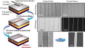
Photolithography is the most widely used lithography technique for commercial fabrication of micro-devices as well as for research and development purposes. However, to perform photolithography, we need a photomask containing the desired pattern. Conventional methods of photomask fabrication involve either photolithography using a direct laser writer or electron-beam lithography. Interestingly, the rise of sequential write scanning probe lithography (SPL) techniques has given rise to various novel methods of direct photomask writing. In this study, we focus on photomask fabrication using a SPL technique, known as ‘Electrolithography’ (ELG), with which multi-scale features can be easily patterned. This is a subtractive lithography technique that involves direct patterning on chromium (Cr) thin films. Being an electrical and direct-write process, ELG bypasses the need for high-power UV laser, electron gun, and polymer resist layers thereby making the process cost-effective and carbon-efficient. We propose a resistless, reliable and novel photomask fabrication process, using the ELG technique, based on a bimetallic architecture. Using the proposed method, we were able to obtain lines having a width of <2 μm, in the best case, and lines with a width < 10 μm repeatedly. We were also able to transfer the fabricated patterns reliably and repeatedly onto a material of choice.