厘米级二维ReS2xSe2(1-x)合金薄膜的可控生长和光电探测器
IF 4.6
3区 工程技术
Q2 ENGINEERING, ELECTRICAL & ELECTRONIC
引用次数: 0
摘要
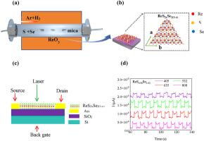
二维(2D)过渡金属二硫族化合物(TMDs)的带隙工程对于推进纳米电子和光电子应用至关重要。合金化具有不同带隙的tmd可以通过成分控制实现精确的带隙调谐。在这项工作中,通过化学气相沉积(CVD),通过改变S/Se前驱体比,成功地在云母衬底上生长了具有可调硫含量(x)的厘米级2D ReS2xSe2(1-x)合金薄膜。ReS2xSe2(1-x)合金薄膜是晶粒尺寸在几纳米到几十纳米之间的多晶薄膜。用这些合金制备的背门控场效应晶体管(fet)表现出与成分相关的电学性能:纯ReS2表现为n型导电行为,而纯ReS2和ReS2xSe2(1-x)合金表现为p型导电行为,ReS0.98Se1.02的空穴迁移率最高,为2.6 cm2/(V·s)。在Au电极和合金通道之间形成欧姆接触。基于这些合金的光电探测器显示了从紫外可见范围到近红外范围的成分可调的光谱响应。S含量为2x >; 1的合金在532 nm和635 nm处表现出最佳的光响应性,而S含量为2x >; 1的合金在405 nm处表现出优异的光响应性。基于ReS1.82Se0.18的光电探测器在405 nm光照射下的光响应率为0.06 AW-1,上升/衰减时间为0.30/0.10 s,而基于res0.98 se1.02的光电探测器在532和635 nm光照射下的光响应率分别为0.02和0.02 AW-1,上升/衰减时间分别为0.16/0.16和0.14/0.12 s。这种趋势与合金的成分可调带隙直接相关。这项工作推进了ReS2xSe2(1-x)薄膜的可扩展合成,并展示了它们在波长选择光电应用方面的潜力。本文章由计算机程序翻译,如有差异,请以英文原文为准。
Controllable growth and photodetectors of centimeter-scale 2D ReS2xSe2(1-x) alloy films
Band-gap engineering in two-dimensional (2D) transition metal dichalcogenides (TMDs) is crucial for advancing nanoelectronics and optoelectronic applications. Alloying TMDs with different band gaps enable precise bandgap tuning through compositional control. In this work, centimeter-scale 2D ReS2xSe2(1-x) alloy films with a tunable sulfur content (x) were successfully grown on mica substrates via chemical vapor deposition (CVD) by varying the S/Se precursor ratio. The ReS2xSe2(1-x) alloy films are polycrystalline films with grain sizes of several nanometers to several tens of nanometers. The back-gated field-effect transistors (FETs) fabricated from these alloys exhibited composition-dependent electrical properties: pure ReS2 exhibited n-type conduction behavior, whereas pure ReSe2 and ReS2xSe2(1-x) alloys exhibited p-type conduction behavior, with ReS0.98Se1.02 achieving the highest hole mobility of 2.6 cm2/(V·s). An ohmic contact was formed between the Au electrodes and alloy channels. Photodetectors based on these alloys displayed composition-tunable spectral responses from the ultraviolet–visible range to the near-infrared range. The alloys with a S content of 2x < 1 exhibited optimal photoresponsivity at 532 nm and 635 nm, whereas those with S composition of 2x > 1 showed superior performance at 405 nm. Photodetectors based on ReS1.82Se0.18 have a photoresponsivity of 0.06 AW-1 and rise/decay times of 0.30/0.10 s under 405 nm light irradiation, respectively, whereas the ReS0.98Se1.02-based device has photoresponsivities of 0.02 and 0.02 AW-1 and rise/decay times of 0.16/0.16 and 0.14/0.12 s under 532 and 635 nm light irradiation, respectively. This trend directly correlates with the composition-tunable bandgap of the alloys. This work advances the scalable synthesis of ReS2xSe2(1-x) films and demonstrates their potential for wavelength-selective optoelectronic applications.
求助全文
通过发布文献求助,成功后即可免费获取论文全文。
去求助
来源期刊

Materials Science in Semiconductor Processing
工程技术-材料科学:综合
CiteScore
8.00
自引率
4.90%
发文量
780
审稿时长
42 days
期刊介绍:
Materials Science in Semiconductor Processing provides a unique forum for the discussion of novel processing, applications and theoretical studies of functional materials and devices for (opto)electronics, sensors, detectors, biotechnology and green energy.
Each issue will aim to provide a snapshot of current insights, new achievements, breakthroughs and future trends in such diverse fields as microelectronics, energy conversion and storage, communications, biotechnology, (photo)catalysis, nano- and thin-film technology, hybrid and composite materials, chemical processing, vapor-phase deposition, device fabrication, and modelling, which are the backbone of advanced semiconductor processing and applications.
Coverage will include: advanced lithography for submicron devices; etching and related topics; ion implantation; damage evolution and related issues; plasma and thermal CVD; rapid thermal processing; advanced metallization and interconnect schemes; thin dielectric layers, oxidation; sol-gel processing; chemical bath and (electro)chemical deposition; compound semiconductor processing; new non-oxide materials and their applications; (macro)molecular and hybrid materials; molecular dynamics, ab-initio methods, Monte Carlo, etc.; new materials and processes for discrete and integrated circuits; magnetic materials and spintronics; heterostructures and quantum devices; engineering of the electrical and optical properties of semiconductors; crystal growth mechanisms; reliability, defect density, intrinsic impurities and defects.
 求助内容:
求助内容: 应助结果提醒方式:


