调节氧空位在a-Ga2O3基忆阻器中实现稳定的非易失性开关特性和神经形态计算
IF 4.6
3区 工程技术
Q2 ENGINEERING, ELECTRICAL & ELECTRONIC
引用次数: 0
摘要
氧化镓由于其宽带隙、高击穿电场和优异的热稳定性,作为一种有前途的忆阻器电阻开关(RS)层引起了人们的广泛关注。然而,实际应用仍然受到诸如相对较低的开关比和循环稳定性不足等挑战的阻碍,这些挑战限制了器件的性能和可靠性。其中,非晶Ga2O3 (a-Ga2O3)薄膜作为RS层来构建忆阻器,其中氧空位被精确调节以提高开关性能。氩氧比为40:10的W/a- ga2o3 /Pt器件在RS行为上优于其他比例的器件,表现出更大的开关窗口(~ 103)、更好的保留(104 s)、更快的响应时间(90 μs)、高稳定性和集中的开关电压分布。此外,我们阐明了电传输机制和导电丝(CFs)模型负责提高开关性能。更令人鼓舞的是,在混合国家标准与技术研究所的图像识别任务中,a-Ga2O3器件达到了98.67%的准确率。这项工作为基于a- ga2o3的记忆电阻器提供了深入的探索,为存储和神经形态计算应用中的开关材料提供了一条有前途的途径。本文章由计算机程序翻译,如有差异,请以英文原文为准。
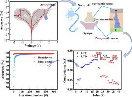
Regulating oxygen vacancies to achieve stable non-volatile switching characteristics and neuromorphic computing in a-Ga2O3 based memristors
Gallium oxide has attracted considerable interest as a promising resistive switching (RS) layer for memristors, owing to its wide bandgap, high breakdown electric field, and excellent thermal stability. However, practical adoption remains hindered by challenges such as relatively low switching ratio and insufficient cycling stability, which limit device performance and reliability. Herein, amorphous Ga2O3 (a-Ga2O3) films serve as the RS layer to construct the memristors, where oxygen vacancies are precisely regulated to enhance the switching performance. The W/a-Ga2O3/Pt device fabricated with an argon-to-oxygen ratio of 40:10 outperforms those made with other ratios in RS behaviors, demonstrating a larger switching window (∼103), superior retention (104 s), faster response times (90 μs), high stability, and concentrated distributions of switching voltages. Furthermore, we elucidate the electrical transport mechanisms and conductive filaments (CFs) models responsible for the enhanced switching performance. More encouragingly, the a-Ga2O3 device achieved up to 98.67 % accuracy on the Mixed National Institute of Standards and Technology image recognition task. This work provides an in-depth exploration of a-Ga2O3-based memristors, offering a promising avenue for switching materials in storage and neuromorphic computing applications.
求助全文
通过发布文献求助,成功后即可免费获取论文全文。
去求助
来源期刊

Materials Science in Semiconductor Processing
工程技术-材料科学:综合
CiteScore
8.00
自引率
4.90%
发文量
780
审稿时长
42 days
期刊介绍:
Materials Science in Semiconductor Processing provides a unique forum for the discussion of novel processing, applications and theoretical studies of functional materials and devices for (opto)electronics, sensors, detectors, biotechnology and green energy.
Each issue will aim to provide a snapshot of current insights, new achievements, breakthroughs and future trends in such diverse fields as microelectronics, energy conversion and storage, communications, biotechnology, (photo)catalysis, nano- and thin-film technology, hybrid and composite materials, chemical processing, vapor-phase deposition, device fabrication, and modelling, which are the backbone of advanced semiconductor processing and applications.
Coverage will include: advanced lithography for submicron devices; etching and related topics; ion implantation; damage evolution and related issues; plasma and thermal CVD; rapid thermal processing; advanced metallization and interconnect schemes; thin dielectric layers, oxidation; sol-gel processing; chemical bath and (electro)chemical deposition; compound semiconductor processing; new non-oxide materials and their applications; (macro)molecular and hybrid materials; molecular dynamics, ab-initio methods, Monte Carlo, etc.; new materials and processes for discrete and integrated circuits; magnetic materials and spintronics; heterostructures and quantum devices; engineering of the electrical and optical properties of semiconductors; crystal growth mechanisms; reliability, defect density, intrinsic impurities and defects.
 求助内容:
求助内容: 应助结果提醒方式:


