Al77Cu20Ti3钎料钎焊55% SiCp/ZL102复合接头的显微组织演变及残余应力分布

IF 4.6 3区 工程技术 Q2 ENGINEERING, ELECTRICAL & ELECTRONIC
Siyan Fan, Dongfeng Cheng
{"title":"Al77Cu20Ti3钎料钎焊55% SiCp/ZL102复合接头的显微组织演变及残余应力分布","authors":"Siyan Fan,&nbsp;Dongfeng Cheng","doi":"10.1016/j.mssp.2025.109987","DOIUrl":null,"url":null,"abstract":"<div><div>In this study, the 55 % SiCp/ZL102 composite was connected by the Al<sub>77</sub>Cu<sub>20</sub>Ti<sub>3</sub> filler through vacuum brazing. The effect of the holding time on the microstructure evolution and mechanical properties of brazed joints was investigated. It was found that with the extension of the holding time, the reactants in the weld were increased, and the Ti-Al-Si ternary compound was the main compound in the weld. The Si element mainly came from the diffusion of the matrix alloy. The maximum shear strength of 81 MPa was obtained for joints brazed at 590 °C for 45 min. The fracture is distributed with tear ridges and tongue-like patterns, which is quasi-cleavage fracture. The finite element software ABAQUS was used to simulate the residual stress of the brazed joint. The simulation results showed that the mismatch of deformation degree between the filler and the base metal caused residual stress concentrated in the brazing seam.</div></div>","PeriodicalId":18240,"journal":{"name":"Materials Science in Semiconductor Processing","volume":"200 ","pages":"Article 109987"},"PeriodicalIF":4.6000,"publicationDate":"2025-08-22","publicationTypes":"Journal Article","fieldsOfStudy":null,"isOpenAccess":false,"openAccessPdf":"","citationCount":"0","resultStr":"{\"title\":\"Microstructural evolution and residual stress distribution of 55 % SiCp/ZL102 composite joint brazed with Al77Cu20Ti3 filler\",\"authors\":\"Siyan Fan,&nbsp;Dongfeng Cheng\",\"doi\":\"10.1016/j.mssp.2025.109987\",\"DOIUrl\":null,\"url\":null,\"abstract\":\"<div><div>In this study, the 55 % SiCp/ZL102 composite was connected by the Al<sub>77</sub>Cu<sub>20</sub>Ti<sub>3</sub> filler through vacuum brazing. The effect of the holding time on the microstructure evolution and mechanical properties of brazed joints was investigated. It was found that with the extension of the holding time, the reactants in the weld were increased, and the Ti-Al-Si ternary compound was the main compound in the weld. The Si element mainly came from the diffusion of the matrix alloy. The maximum shear strength of 81 MPa was obtained for joints brazed at 590 °C for 45 min. The fracture is distributed with tear ridges and tongue-like patterns, which is quasi-cleavage fracture. The finite element software ABAQUS was used to simulate the residual stress of the brazed joint. The simulation results showed that the mismatch of deformation degree between the filler and the base metal caused residual stress concentrated in the brazing seam.</div></div>\",\"PeriodicalId\":18240,\"journal\":{\"name\":\"Materials Science in Semiconductor Processing\",\"volume\":\"200 \",\"pages\":\"Article 109987\"},\"PeriodicalIF\":4.6000,\"publicationDate\":\"2025-08-22\",\"publicationTypes\":\"Journal Article\",\"fieldsOfStudy\":null,\"isOpenAccess\":false,\"openAccessPdf\":\"\",\"citationCount\":\"0\",\"resultStr\":null,\"platform\":\"Semanticscholar\",\"paperid\":null,\"PeriodicalName\":\"Materials Science in Semiconductor Processing\",\"FirstCategoryId\":\"5\",\"ListUrlMain\":\"https://www.sciencedirect.com/science/article/pii/S1369800125007243\",\"RegionNum\":3,\"RegionCategory\":\"工程技术\",\"ArticlePicture\":[],\"TitleCN\":null,\"AbstractTextCN\":null,\"PMCID\":null,\"EPubDate\":\"\",\"PubModel\":\"\",\"JCR\":\"Q2\",\"JCRName\":\"ENGINEERING, ELECTRICAL & ELECTRONIC\",\"Score\":null,\"Total\":0}","platform":"Semanticscholar","paperid":null,"PeriodicalName":"Materials Science in Semiconductor Processing","FirstCategoryId":"5","ListUrlMain":"https://www.sciencedirect.com/science/article/pii/S1369800125007243","RegionNum":3,"RegionCategory":"工程技术","ArticlePicture":[],"TitleCN":null,"AbstractTextCN":null,"PMCID":null,"EPubDate":"","PubModel":"","JCR":"Q2","JCRName":"ENGINEERING, ELECTRICAL & ELECTRONIC","Score":null,"Total":0}
引用次数: 0

摘要

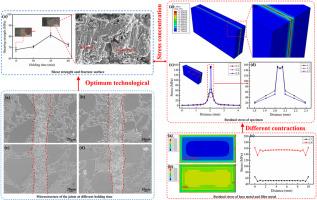
本研究采用Al77Cu20Ti3填料真空钎焊连接55% SiCp/ZL102复合材料。研究了保温时间对钎焊接头组织演变和力学性能的影响。结果发现,随着保温时间的延长,焊缝中的反应物增多,且以Ti-Al-Si三元化合物为主。Si元素主要来源于基体合金的扩散。在590℃下钎焊45 min,接头的最大抗剪强度为81 MPa。断口呈撕裂脊状,呈舌状,属准解理断裂。采用有限元软件ABAQUS对钎焊接头的残余应力进行了模拟。模拟结果表明,钎料与母材变形程度不匹配导致残余应力集中在钎焊缝内。
本文章由计算机程序翻译,如有差异,请以英文原文为准。

Microstructural evolution and residual stress distribution of 55 % SiCp/ZL102 composite joint brazed with Al77Cu20Ti3 filler

Microstructural evolution and residual stress distribution of 55 % SiCp/ZL102 composite joint brazed with Al77Cu20Ti3 filler
In this study, the 55 % SiCp/ZL102 composite was connected by the Al77Cu20Ti3 filler through vacuum brazing. The effect of the holding time on the microstructure evolution and mechanical properties of brazed joints was investigated. It was found that with the extension of the holding time, the reactants in the weld were increased, and the Ti-Al-Si ternary compound was the main compound in the weld. The Si element mainly came from the diffusion of the matrix alloy. The maximum shear strength of 81 MPa was obtained for joints brazed at 590 °C for 45 min. The fracture is distributed with tear ridges and tongue-like patterns, which is quasi-cleavage fracture. The finite element software ABAQUS was used to simulate the residual stress of the brazed joint. The simulation results showed that the mismatch of deformation degree between the filler and the base metal caused residual stress concentrated in the brazing seam.
求助全文
通过发布文献求助,成功后即可免费获取论文全文。 去求助
来源期刊
Materials Science in Semiconductor Processing
Materials Science in Semiconductor Processing 工程技术-材料科学:综合
CiteScore
8.00
自引率
4.90%
发文量
780
审稿时长
42 days
期刊介绍: Materials Science in Semiconductor Processing provides a unique forum for the discussion of novel processing, applications and theoretical studies of functional materials and devices for (opto)electronics, sensors, detectors, biotechnology and green energy. Each issue will aim to provide a snapshot of current insights, new achievements, breakthroughs and future trends in such diverse fields as microelectronics, energy conversion and storage, communications, biotechnology, (photo)catalysis, nano- and thin-film technology, hybrid and composite materials, chemical processing, vapor-phase deposition, device fabrication, and modelling, which are the backbone of advanced semiconductor processing and applications. Coverage will include: advanced lithography for submicron devices; etching and related topics; ion implantation; damage evolution and related issues; plasma and thermal CVD; rapid thermal processing; advanced metallization and interconnect schemes; thin dielectric layers, oxidation; sol-gel processing; chemical bath and (electro)chemical deposition; compound semiconductor processing; new non-oxide materials and their applications; (macro)molecular and hybrid materials; molecular dynamics, ab-initio methods, Monte Carlo, etc.; new materials and processes for discrete and integrated circuits; magnetic materials and spintronics; heterostructures and quantum devices; engineering of the electrical and optical properties of semiconductors; crystal growth mechanisms; reliability, defect density, intrinsic impurities and defects.
×
引用
GB/T 7714-2015
复制
MLA
复制
APA
复制
导出至
BibTeX EndNote RefMan NoteFirst NoteExpress
×
提示
您的信息不完整,为了账户安全,请先补充。
现在去补充
×
提示
您因"违规操作"
具体请查看互助需知
我知道了
×
提示
确定
请完成安全验证×
copy
已复制链接
快去分享给好友吧!
我知道了
右上角分享
点击右上角分享
0
联系我们:info@booksci.cn Book学术提供免费学术资源搜索服务,方便国内外学者检索中英文文献。致力于提供最便捷和优质的服务体验。 Copyright © 2023 布克学术 All rights reserved.
京ICP备2023020795号-1
ghs 京公网安备 11010802042870号
Book学术文献互助
Book学术文献互助群
群 号:604180095
Book学术官方微信