具有铼型肖特基触点的MIS器件的负电容和负介电行为

IF 1.4 4区 物理与天体物理 Q3 ENGINEERING, ELECTRICAL & ELECTRONIC
Mehmet İzzeddin Güler , Ahmet Kaymaz , Esra Evcin-Baydilli , Haziret Durmuş , Şemsettin Altındal
{"title":"具有铼型肖特基触点的MIS器件的负电容和负介电行为","authors":"Mehmet İzzeddin Güler ,&nbsp;Ahmet Kaymaz ,&nbsp;Esra Evcin-Baydilli ,&nbsp;Haziret Durmuş ,&nbsp;Şemsettin Altındal","doi":"10.1016/j.sse.2025.109204","DOIUrl":null,"url":null,"abstract":"<div><div>This study offers a thorough examination of the negative capacitance/dielectric behavior of an MIS device with rhenium (Re) type Schottky contact and native oxide interlayer. The pulsed laser deposition method was used to deposit Re as the Schottky contact on the n-type GaAs substrates. Thus, the electrical and dielectric properties were evaluated by <em>I-V, C-V,</em> and <em>G/ω-V</em> tests at<!--> <!-->a high frequency (1 MHz). Experimental results demonstrated that capacitance characteristics showed a marked increase from the inversion region to depletion, with a localized peak observed at 0.26 V. Exceeding 4.16 V, the capacitance values turn negative, signifying a shift to inductive behavior, as shown by a rapid increase in conductance values under the same conditions. In addition, the dynamic resistance profile indicates that the series resistance (<em>R<sub>s</sub></em>) reaches its peak at near-zero bias and stabilizes under significant forward bias, approaching the device’s intrinsic series resistance. Analysis of the <em>C–G/ω–V</em> data also showed two distinct peaks in the corrected conductance (<em>Gc/ω</em>) at –0.55  V and + 0.1  V, due to the response of interface states (<em>N<sub>ss</sub></em>) located at distinct energy levels inside the GaAs bandgap. The transition from capacitive to inductive behavior was recorded with high enough forward bias, at which point the dielectric constant (<em>ε′</em>) turns negative, showing the effects of polarization reversal and reactive energy storage. Additionally, the complex impedance analysis revealed distorted semicircular arcs and loop formations, indicative of interfacial inhomogeneities and multiple charge transport channels. As a result, these findings demonstrate that integrating Re into the MIS structure significantly improves the device’s electrical stability and functional response under varying bias conditions, demonstrating its potential in advanced high-frequency and low-power electronic applications.</div></div>","PeriodicalId":21909,"journal":{"name":"Solid-state Electronics","volume":"229 ","pages":"Article 109204"},"PeriodicalIF":1.4000,"publicationDate":"2025-08-12","publicationTypes":"Journal Article","fieldsOfStudy":null,"isOpenAccess":false,"openAccessPdf":"","citationCount":"0","resultStr":"{\"title\":\"Negative capacitance and negative dielectric behavior of MIS device with Rhenium-Type Schottky contacts\",\"authors\":\"Mehmet İzzeddin Güler ,&nbsp;Ahmet Kaymaz ,&nbsp;Esra Evcin-Baydilli ,&nbsp;Haziret Durmuş ,&nbsp;Şemsettin Altındal\",\"doi\":\"10.1016/j.sse.2025.109204\",\"DOIUrl\":null,\"url\":null,\"abstract\":\"<div><div>This study offers a thorough examination of the negative capacitance/dielectric behavior of an MIS device with rhenium (Re) type Schottky contact and native oxide interlayer. The pulsed laser deposition method was used to deposit Re as the Schottky contact on the n-type GaAs substrates. Thus, the electrical and dielectric properties were evaluated by <em>I-V, C-V,</em> and <em>G/ω-V</em> tests at<!--> <!-->a high frequency (1 MHz). Experimental results demonstrated that capacitance characteristics showed a marked increase from the inversion region to depletion, with a localized peak observed at 0.26 V. Exceeding 4.16 V, the capacitance values turn negative, signifying a shift to inductive behavior, as shown by a rapid increase in conductance values under the same conditions. In addition, the dynamic resistance profile indicates that the series resistance (<em>R<sub>s</sub></em>) reaches its peak at near-zero bias and stabilizes under significant forward bias, approaching the device’s intrinsic series resistance. Analysis of the <em>C–G/ω–V</em> data also showed two distinct peaks in the corrected conductance (<em>Gc/ω</em>) at –0.55  V and + 0.1  V, due to the response of interface states (<em>N<sub>ss</sub></em>) located at distinct energy levels inside the GaAs bandgap. The transition from capacitive to inductive behavior was recorded with high enough forward bias, at which point the dielectric constant (<em>ε′</em>) turns negative, showing the effects of polarization reversal and reactive energy storage. Additionally, the complex impedance analysis revealed distorted semicircular arcs and loop formations, indicative of interfacial inhomogeneities and multiple charge transport channels. As a result, these findings demonstrate that integrating Re into the MIS structure significantly improves the device’s electrical stability and functional response under varying bias conditions, demonstrating its potential in advanced high-frequency and low-power electronic applications.</div></div>\",\"PeriodicalId\":21909,\"journal\":{\"name\":\"Solid-state Electronics\",\"volume\":\"229 \",\"pages\":\"Article 109204\"},\"PeriodicalIF\":1.4000,\"publicationDate\":\"2025-08-12\",\"publicationTypes\":\"Journal Article\",\"fieldsOfStudy\":null,\"isOpenAccess\":false,\"openAccessPdf\":\"\",\"citationCount\":\"0\",\"resultStr\":null,\"platform\":\"Semanticscholar\",\"paperid\":null,\"PeriodicalName\":\"Solid-state Electronics\",\"FirstCategoryId\":\"101\",\"ListUrlMain\":\"https://www.sciencedirect.com/science/article/pii/S0038110125001492\",\"RegionNum\":4,\"RegionCategory\":\"物理与天体物理\",\"ArticlePicture\":[],\"TitleCN\":null,\"AbstractTextCN\":null,\"PMCID\":null,\"EPubDate\":\"\",\"PubModel\":\"\",\"JCR\":\"Q3\",\"JCRName\":\"ENGINEERING, ELECTRICAL & ELECTRONIC\",\"Score\":null,\"Total\":0}","platform":"Semanticscholar","paperid":null,"PeriodicalName":"Solid-state Electronics","FirstCategoryId":"101","ListUrlMain":"https://www.sciencedirect.com/science/article/pii/S0038110125001492","RegionNum":4,"RegionCategory":"物理与天体物理","ArticlePicture":[],"TitleCN":null,"AbstractTextCN":null,"PMCID":null,"EPubDate":"","PubModel":"","JCR":"Q3","JCRName":"ENGINEERING, ELECTRICAL & ELECTRONIC","Score":null,"Total":0}
引用次数: 0

摘要

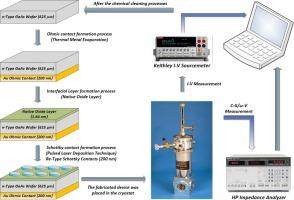
本研究对具有铼(Re)型肖特基触点和天然氧化物中间层的MIS器件的负电容/介电行为进行了全面的研究。采用脉冲激光沉积法在n型GaAs衬底上沉积了作为肖特基触点的Re。因此,在高频(1 MHz)下,通过I-V、C-V和G/ω-V测试来评估电学和介电性能。实验结果表明,从反转区到耗尽区,电容特性显著增加,在0.26 V处出现局域峰值。超过4.16 V时,电容值变为负值,表明转向电感行为,在相同条件下电导值迅速增加。此外,动态电阻曲线表明,串联电阻(Rs)在接近零偏置时达到峰值,在显著的正向偏置下趋于稳定,接近器件的固有串联电阻。对C-G /ω - V数据的分析也显示,校正后的电导(Gc/ω)在-0.55 V和+ 0.1 V处有两个明显的峰,这是由于GaAs带隙内不同能级的界面态(Nss)的响应。当正向偏压足够大时,记录了从电容性到电感性的转变,此时介电常数(ε’)变为负值,显示了极化反转和无功能量存储的影响。此外,复合阻抗分析还发现了扭曲的半圆弧和环形结构,表明界面不均匀性和多个电荷传输通道。因此,这些研究结果表明,将Re集成到MIS结构中可以显着提高设备在不同偏置条件下的电气稳定性和功能响应,从而展示了其在先进高频和低功耗电子应用中的潜力。
本文章由计算机程序翻译,如有差异,请以英文原文为准。

Negative capacitance and negative dielectric behavior of MIS device with Rhenium-Type Schottky contacts

Negative capacitance and negative dielectric behavior of MIS device with Rhenium-Type Schottky contacts
This study offers a thorough examination of the negative capacitance/dielectric behavior of an MIS device with rhenium (Re) type Schottky contact and native oxide interlayer. The pulsed laser deposition method was used to deposit Re as the Schottky contact on the n-type GaAs substrates. Thus, the electrical and dielectric properties were evaluated by I-V, C-V, and G/ω-V tests at a high frequency (1 MHz). Experimental results demonstrated that capacitance characteristics showed a marked increase from the inversion region to depletion, with a localized peak observed at 0.26 V. Exceeding 4.16 V, the capacitance values turn negative, signifying a shift to inductive behavior, as shown by a rapid increase in conductance values under the same conditions. In addition, the dynamic resistance profile indicates that the series resistance (Rs) reaches its peak at near-zero bias and stabilizes under significant forward bias, approaching the device’s intrinsic series resistance. Analysis of the C–G/ω–V data also showed two distinct peaks in the corrected conductance (Gc/ω) at –0.55  V and + 0.1  V, due to the response of interface states (Nss) located at distinct energy levels inside the GaAs bandgap. The transition from capacitive to inductive behavior was recorded with high enough forward bias, at which point the dielectric constant (ε′) turns negative, showing the effects of polarization reversal and reactive energy storage. Additionally, the complex impedance analysis revealed distorted semicircular arcs and loop formations, indicative of interfacial inhomogeneities and multiple charge transport channels. As a result, these findings demonstrate that integrating Re into the MIS structure significantly improves the device’s electrical stability and functional response under varying bias conditions, demonstrating its potential in advanced high-frequency and low-power electronic applications.
求助全文
通过发布文献求助,成功后即可免费获取论文全文。 去求助
来源期刊
Solid-state Electronics
Solid-state Electronics 物理-工程:电子与电气
CiteScore
3.00
自引率
5.90%
发文量
212
审稿时长
3 months
期刊介绍: It is the aim of this journal to bring together in one publication outstanding papers reporting new and original work in the following areas: (1) applications of solid-state physics and technology to electronics and optoelectronics, including theory and device design; (2) optical, electrical, morphological characterization techniques and parameter extraction of devices; (3) fabrication of semiconductor devices, and also device-related materials growth, measurement and evaluation; (4) the physics and modeling of submicron and nanoscale microelectronic and optoelectronic devices, including processing, measurement, and performance evaluation; (5) applications of numerical methods to the modeling and simulation of solid-state devices and processes; and (6) nanoscale electronic and optoelectronic devices, photovoltaics, sensors, and MEMS based on semiconductor and alternative electronic materials; (7) synthesis and electrooptical properties of materials for novel devices.
×
引用
GB/T 7714-2015
复制
MLA
复制
APA
复制
导出至
BibTeX EndNote RefMan NoteFirst NoteExpress
×
提示
您的信息不完整,为了账户安全,请先补充。
现在去补充
×
提示
您因"违规操作"
具体请查看互助需知
我知道了
×
提示
确定
请完成安全验证×
copy
已复制链接
快去分享给好友吧!
我知道了
右上角分享
点击右上角分享
0
联系我们:info@booksci.cn Book学术提供免费学术资源搜索服务,方便国内外学者检索中英文文献。致力于提供最便捷和优质的服务体验。 Copyright © 2023 布克学术 All rights reserved.
京ICP备2023020795号-1
ghs 京公网安备 11010802042870号
Book学术文献互助
Book学术文献互助群
群 号:604180095
Book学术官方微信