通过扫描电镜图像的计算分析来测量粗糙基底上薄涂层的厚度
IF 3.1
Q2 ENGINEERING, ELECTRICAL & ELECTRONIC
引用次数: 0
摘要
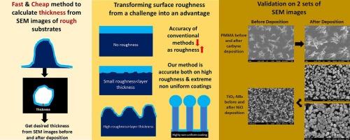
本文介绍了一种计算方法,通过分析自顶向下扫描电子显微镜(SEM)图像来量化沉积在高度粗糙衬底上的薄膜厚度。该方法需要测量沉积前后获得的粗糙表面的自上而下SEM图像的亮区,通过沉积引起的亮区增强与沉积前后这些区域的平均周长的比值来预测薄膜厚度。该技术通过具有预定义薄膜厚度的合成SEM图像进行了验证,并结合了通过扩散限制聚集(DLA)模拟生成的简单和复杂的衬底形态,以增加真实感。通过分析涂有碳炔的等离子蚀刻聚合物(PMMA)表面和涂有NiO的TiO2纳米棒的SEM图像,探索了实验应用,证明了该方法在不同表面粗糙度和形貌下的有效性。这项工作为未来的发展奠定了基础,包括在合成数据集上训练的神经网络的实现,以提高粗糙基材涂层厚度的测量精度,以及通过扫描电镜图像分析重建金属层溅射之前的真实表面形态。本文章由计算机程序翻译,如有差异,请以英文原文为准。
Measurement of thickness of thin coatings on rough substrates via computational analysis of SEM images
This work introduces a computational method to quantify the thickness of thin films deposited on highly rough substrates analyzing top-down Scanning Electron Microscope (SEM) images. The method entails measuring the bright areas of top-down SEM images of the rough surface obtained before and after deposition, allowing for the prediction of film thickness through the ratio of bright area enhancement caused by deposition to the average perimeter of these areas before and after deposition. Validation of this technique was conducted via synthetic SEM images with predefined film thicknesses, incorporating simple and complex substrate morphologies generated through Diffusion-Limited Aggregation (DLA) simulations for added realism. Experimental applications were explored through the analysis of SEM images of plasma-etched polymer (PMMA) surfaces coated with carbyne and of nanorods of TiO2 coated with NiO, demonstrating the method's efficacy across varying surface roughness and morphologies. This work lays the foundation for future advancements, including the implementation of a neural network trained on synthetic datasets to enhance the measurement accuracy of coating thickness on rough substrates as well as the reconstruction of true surface morphologies prior to metal layer sputtering via SEM image analysis.
求助全文
通过发布文献求助,成功后即可免费获取论文全文。
去求助
来源期刊
Micro and Nano Engineering
Engineering-Electrical and Electronic Engineering
CiteScore
3.30
自引率
0.00%
发文量
67
审稿时长
80 days
 求助内容:
求助内容: 应助结果提醒方式:


