等离子体修饰诱导界面工程增强了具有超高性能和偏置选择性响应的GaN紫外光电探测器
IF 9.7
2区 材料科学
Q1 MATERIALS SCIENCE, MULTIDISCIPLINARY
引用次数: 0
摘要
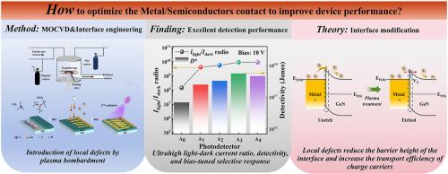
接口组装缺陷通常会导致相当大的漏电流和器件性能下降,因此,接口工程策略已经成为器件制造的一个关键方面。本文采用单面等离子体刻蚀法修饰金属/半导体(M/S)界面,制备了非对称M/S接触式gan基光电探测器(PD)。与未经处理的氮化镓基PD相比,经过界面工程处理的氮化镓基PD具有超高的光暗电流比9.35 × 109和5.64 × 10¹⁷ Jones的高探测率。即使考虑噪声影响,探测值仍然很高,约为1016琼斯,这与光电倍增管相当。等离子体处理钝化了GaN界面悬垂键,而蚀刻引起的局域N空位在GaN能带结构中起到浅层供体能级的作用,降低了界面的势垒高度,提高了载流子的输运效率。此外,通过影响M/S接口的耗尽层宽度,器件获得偏置调谐的选择性响应(UVC、UV-C到a、UVA波段),可以满足各种应用需求。因此,通过接口工程有意引入局部缺陷是优化器件性能的有效策略,同时也为今后的器件设计提供了参考。本文章由计算机程序翻译,如有差异,请以英文原文为准。
Plasma modification induced interface engineering enhanced GaN UV photodetectors with ultrahigh performance and bias-tuned selective response
Deficient assembly of interfaces often results in considerable leakage current and compromised device performance, therefore, interface engineering strategy has emerged as a crucial aspect of device fabrication. In this work, the metal/semiconductor (M/S) interface was modified by single-sided plasma etching to fabricate an asymmetric M/S contact GaN-based photodetector (PD). Compared to untreated GaN-based PD, the GaN-based PD with interface engineering exhibits superior performance with an ultrahigh light-dark current ratio of 9.35 × 10⁹ and a high detectivity of 5.64 × 10¹⁷ Jones. Even considering noise effects, the detectivity value remains high at ∼1016 Jones, which is comparable to photomultiplier tubes. The performance improvement is attributed to the passivation of GaN interface dangling bonds by plasma treatment, while the localized N vacancies induced by etching act as shallow donor energy levels in the GaN energy band structure, reducing the barrier height of the interface and increasing the transport efficiency of charge carriers. In addition, by affecting the depletion layer width of the M/S interface, the device gains a bias-tuned selective response (UVC, UV-C to A, UVA waveband), which can meet various application requirements. Consequently, intentionally introducing local defects via interface engineering is an efficient strategy to optimize device performance while serving as a reference for future device design.
求助全文
通过发布文献求助,成功后即可免费获取论文全文。
去求助
来源期刊
Materials Today Physics
Materials Science-General Materials Science
CiteScore
14.00
自引率
7.80%
发文量
284
审稿时长
15 days
期刊介绍:
Materials Today Physics is a multi-disciplinary journal focused on the physics of materials, encompassing both the physical properties and materials synthesis. Operating at the interface of physics and materials science, this journal covers one of the largest and most dynamic fields within physical science. The forefront research in materials physics is driving advancements in new materials, uncovering new physics, and fostering novel applications at an unprecedented pace.
 求助内容:
求助内容: 应助结果提醒方式:


