Yan Tian, Hao Liu, Jiaming Guo, Jing Li, Baodan Liu and Fei Liu
{"title":"设计一种先进的WS2/a-Ga2O3高温光电探测器†","authors":"Yan Tian, Hao Liu, Jiaming Guo, Jing Li, Baodan Liu and Fei Liu","doi":"10.1039/D5TC01338K","DOIUrl":null,"url":null,"abstract":"<p >High-temperature photodetectors have attracted tremendous attention in recent years due to their potential applications in very large-scale integration (VLSI), industrial manufacturing and aerospace exploration. However, current high-temperature photodetectors usually encounter some challenges, such as complex device structures, low photoresponsivity and poor stability. In this study, a centimeter-scale, ultrathin amorphous gallium oxide (a-Ga<small><sub>2</sub></small>O<small><sub>3</sub></small>) film is used for the first time as a heat insulation layer to improve the high-temperature performance of a multilayer WS<small><sub>2</sub></small> photodetector. With the help of the a-Ga<small><sub>2</sub></small>O<small><sub>3</sub></small> layer with high heat resistance, the WS<small><sub>2</sub></small> photodetector achieves a high photoresponsivity of 73.8 A W<small><sup>−1</sup></small> at 155 °C, surpassing most other 2D-nanomaterial-based photodetectors. More interestingly, the response time is reduced to 22.9 ms and the specific detectivity reaches as much as 6.64 × 10<small><sup>10</sup></small> Jones, values which are much better than those of a WS<small><sub>2</sub></small>/SiO<small><sub>2</sub></small> device (39 ms, 2.87 × 10<small><sup>7</sup></small> Jones) at 125 °C. The WS<small><sub>2</sub></small>/a-Ga<small><sub>2</sub></small>O<small><sub>3</sub></small> nanodevice has successfully solved the trade-off between device stability and device performance of the photodetector at high temperature, which can be ascribed to the use of the a-Ga<small><sub>2</sub></small>O<small><sub>3</sub></small> film, which can simultaneously enhance the separation efficiency of photogenerated carriers and suppress thermal diffusion from a high-temperature substrate. Our research may provide an efficient strategy to promote the high-temperature applications of 2D-material-based photodetectors.</p>","PeriodicalId":84,"journal":{"name":"Journal of Materials Chemistry C","volume":" 29","pages":" 15185-15194"},"PeriodicalIF":5.1000,"publicationDate":"2025-06-18","publicationTypes":"Journal Article","fieldsOfStudy":null,"isOpenAccess":false,"openAccessPdf":"","citationCount":"0","resultStr":"{\"title\":\"Devising an advanced WS2/a-Ga2O3 photodetector for high-temperature operation†\",\"authors\":\"Yan Tian, Hao Liu, Jiaming Guo, Jing Li, Baodan Liu and Fei Liu\",\"doi\":\"10.1039/D5TC01338K\",\"DOIUrl\":null,\"url\":null,\"abstract\":\"<p >High-temperature photodetectors have attracted tremendous attention in recent years due to their potential applications in very large-scale integration (VLSI), industrial manufacturing and aerospace exploration. However, current high-temperature photodetectors usually encounter some challenges, such as complex device structures, low photoresponsivity and poor stability. In this study, a centimeter-scale, ultrathin amorphous gallium oxide (a-Ga<small><sub>2</sub></small>O<small><sub>3</sub></small>) film is used for the first time as a heat insulation layer to improve the high-temperature performance of a multilayer WS<small><sub>2</sub></small> photodetector. With the help of the a-Ga<small><sub>2</sub></small>O<small><sub>3</sub></small> layer with high heat resistance, the WS<small><sub>2</sub></small> photodetector achieves a high photoresponsivity of 73.8 A W<small><sup>−1</sup></small> at 155 °C, surpassing most other 2D-nanomaterial-based photodetectors. More interestingly, the response time is reduced to 22.9 ms and the specific detectivity reaches as much as 6.64 × 10<small><sup>10</sup></small> Jones, values which are much better than those of a WS<small><sub>2</sub></small>/SiO<small><sub>2</sub></small> device (39 ms, 2.87 × 10<small><sup>7</sup></small> Jones) at 125 °C. The WS<small><sub>2</sub></small>/a-Ga<small><sub>2</sub></small>O<small><sub>3</sub></small> nanodevice has successfully solved the trade-off between device stability and device performance of the photodetector at high temperature, which can be ascribed to the use of the a-Ga<small><sub>2</sub></small>O<small><sub>3</sub></small> film, which can simultaneously enhance the separation efficiency of photogenerated carriers and suppress thermal diffusion from a high-temperature substrate. Our research may provide an efficient strategy to promote the high-temperature applications of 2D-material-based photodetectors.</p>\",\"PeriodicalId\":84,\"journal\":{\"name\":\"Journal of Materials Chemistry C\",\"volume\":\" 29\",\"pages\":\" 15185-15194\"},\"PeriodicalIF\":5.1000,\"publicationDate\":\"2025-06-18\",\"publicationTypes\":\"Journal Article\",\"fieldsOfStudy\":null,\"isOpenAccess\":false,\"openAccessPdf\":\"\",\"citationCount\":\"0\",\"resultStr\":null,\"platform\":\"Semanticscholar\",\"paperid\":null,\"PeriodicalName\":\"Journal of Materials Chemistry C\",\"FirstCategoryId\":\"1\",\"ListUrlMain\":\"https://pubs.rsc.org/en/content/articlelanding/2025/tc/d5tc01338k\",\"RegionNum\":2,\"RegionCategory\":\"材料科学\",\"ArticlePicture\":[],\"TitleCN\":null,\"AbstractTextCN\":null,\"PMCID\":null,\"EPubDate\":\"\",\"PubModel\":\"\",\"JCR\":\"Q2\",\"JCRName\":\"MATERIALS SCIENCE, MULTIDISCIPLINARY\",\"Score\":null,\"Total\":0}","platform":"Semanticscholar","paperid":null,"PeriodicalName":"Journal of Materials Chemistry C","FirstCategoryId":"1","ListUrlMain":"https://pubs.rsc.org/en/content/articlelanding/2025/tc/d5tc01338k","RegionNum":2,"RegionCategory":"材料科学","ArticlePicture":[],"TitleCN":null,"AbstractTextCN":null,"PMCID":null,"EPubDate":"","PubModel":"","JCR":"Q2","JCRName":"MATERIALS SCIENCE, MULTIDISCIPLINARY","Score":null,"Total":0}
Devising an advanced WS2/a-Ga2O3 photodetector for high-temperature operation†
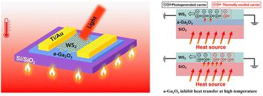
High-temperature photodetectors have attracted tremendous attention in recent years due to their potential applications in very large-scale integration (VLSI), industrial manufacturing and aerospace exploration. However, current high-temperature photodetectors usually encounter some challenges, such as complex device structures, low photoresponsivity and poor stability. In this study, a centimeter-scale, ultrathin amorphous gallium oxide (a-Ga2O3) film is used for the first time as a heat insulation layer to improve the high-temperature performance of a multilayer WS2 photodetector. With the help of the a-Ga2O3 layer with high heat resistance, the WS2 photodetector achieves a high photoresponsivity of 73.8 A W−1 at 155 °C, surpassing most other 2D-nanomaterial-based photodetectors. More interestingly, the response time is reduced to 22.9 ms and the specific detectivity reaches as much as 6.64 × 10¹⁰ Jones, values which are much better than those of a WS2/SiO2 device (39 ms, 2.87 × 10⁷ Jones) at 125 °C. The WS2/a-Ga2O3 nanodevice has successfully solved the trade-off between device stability and device performance of the photodetector at high temperature, which can be ascribed to the use of the a-Ga2O3 film, which can simultaneously enhance the separation efficiency of photogenerated carriers and suppress thermal diffusion from a high-temperature substrate. Our research may provide an efficient strategy to promote the high-temperature applications of 2D-material-based photodetectors.
期刊介绍:
The Journal of Materials Chemistry is divided into three distinct sections, A, B, and C, each catering to specific applications of the materials under study:
Journal of Materials Chemistry A focuses primarily on materials intended for applications in energy and sustainability.
Journal of Materials Chemistry B specializes in materials designed for applications in biology and medicine.
Journal of Materials Chemistry C is dedicated to materials suitable for applications in optical, magnetic, and electronic devices.
Example topic areas within the scope of Journal of Materials Chemistry C are listed below. This list is neither exhaustive nor exclusive.
Bioelectronics
Conductors
Detectors
Dielectrics
Displays
Ferroelectrics
Lasers
LEDs
Lighting
Liquid crystals
Memory
Metamaterials
Multiferroics
Photonics
Photovoltaics
Semiconductors
Sensors
Single molecule conductors
Spintronics
Superconductors
Thermoelectrics
Topological insulators
Transistors

 求助内容:
求助内容: 应助结果提醒方式:


