用于生态友好型热电能量收集的模块级硅3D软化纳米结构

IF 9.7 2区 材料科学 Q1 MATERIALS SCIENCE, MULTIDISCIPLINARY
Ryohei Nagahiro , Bin Xu , Shingo Terashima , Yifei Li , Yuanzhe Li , Yuxuan Liao , Zhenglong Fang , Cheng Shao , Masato Ohnishi , Shinya Kato , Eiji Iwase , Junichiro Shiomi
{"title":"用于生态友好型热电能量收集的模块级硅3D软化纳米结构","authors":"Ryohei Nagahiro ,&nbsp;Bin Xu ,&nbsp;Shingo Terashima ,&nbsp;Yifei Li ,&nbsp;Yuanzhe Li ,&nbsp;Yuxuan Liao ,&nbsp;Zhenglong Fang ,&nbsp;Cheng Shao ,&nbsp;Masato Ohnishi ,&nbsp;Shinya Kato ,&nbsp;Eiji Iwase ,&nbsp;Junichiro Shiomi","doi":"10.1016/j.mtphys.2025.101798","DOIUrl":null,"url":null,"abstract":"<div><div>Widespread of internet-of-things with wireless sensing and transmission devices require self-powering module consisting of abundant and environmental-friendly materials. Si thermoelectric material is a promising candidate and sufficient figure of merit (<span><math><mrow><mi>z</mi><mi>T</mi></mrow></math></span>) has been realized in the form of nanoscale derivatives. However, scaling it up to bulk material while maintaining the <span><math><mrow><mi>z</mi><mi>T</mi></mrow></math></span> has been challenging. This difficulty arises from the lack of scalable nanostructures that effectively impede phonon transport without significantly sacrificing electron transport in the bulk process, which is rooted in the intrinsic trade-off between electrical and thermal transport mechanisms. To overcome this limitation, this study introduces a scalable 3D softened nanoarchitecture by a highly non-equilibrium sintering process, featuring narrow-conduction path between nanograins, which facilitates selective electron/phonon interface transmission due to the induced significant strain. This strain engineering results in remarkable <span><math><mrow><mi>z</mi><mi>T</mi></mrow></math></span> values for both n- and p-type bulk 3D Si nanoarchitectures (0.11–0.23 at room temperature and 0.44–0.67 about 750 K), which are 5–10 times those of previously reported bulk nanostructured Si materials. The superior <span><math><mrow><mi>z</mi><mi>T</mi></mrow></math></span> and scalability enables integrating the Si thermoelectric materials into a flexible module and realized powering wireless sensor devices for 24 h.</div></div>","PeriodicalId":18253,"journal":{"name":"Materials Today Physics","volume":"57 ","pages":"Article 101798"},"PeriodicalIF":9.7000,"publicationDate":"2025-07-12","publicationTypes":"Journal Article","fieldsOfStudy":null,"isOpenAccess":false,"openAccessPdf":"","citationCount":"0","resultStr":"{\"title\":\"Module-scale silicon 3D softened nanoarchitectures for eco-friendly thermoelectric energy harvesting\",\"authors\":\"Ryohei Nagahiro ,&nbsp;Bin Xu ,&nbsp;Shingo Terashima ,&nbsp;Yifei Li ,&nbsp;Yuanzhe Li ,&nbsp;Yuxuan Liao ,&nbsp;Zhenglong Fang ,&nbsp;Cheng Shao ,&nbsp;Masato Ohnishi ,&nbsp;Shinya Kato ,&nbsp;Eiji Iwase ,&nbsp;Junichiro Shiomi\",\"doi\":\"10.1016/j.mtphys.2025.101798\",\"DOIUrl\":null,\"url\":null,\"abstract\":\"<div><div>Widespread of internet-of-things with wireless sensing and transmission devices require self-powering module consisting of abundant and environmental-friendly materials. Si thermoelectric material is a promising candidate and sufficient figure of merit (<span><math><mrow><mi>z</mi><mi>T</mi></mrow></math></span>) has been realized in the form of nanoscale derivatives. However, scaling it up to bulk material while maintaining the <span><math><mrow><mi>z</mi><mi>T</mi></mrow></math></span> has been challenging. This difficulty arises from the lack of scalable nanostructures that effectively impede phonon transport without significantly sacrificing electron transport in the bulk process, which is rooted in the intrinsic trade-off between electrical and thermal transport mechanisms. To overcome this limitation, this study introduces a scalable 3D softened nanoarchitecture by a highly non-equilibrium sintering process, featuring narrow-conduction path between nanograins, which facilitates selective electron/phonon interface transmission due to the induced significant strain. This strain engineering results in remarkable <span><math><mrow><mi>z</mi><mi>T</mi></mrow></math></span> values for both n- and p-type bulk 3D Si nanoarchitectures (0.11–0.23 at room temperature and 0.44–0.67 about 750 K), which are 5–10 times those of previously reported bulk nanostructured Si materials. The superior <span><math><mrow><mi>z</mi><mi>T</mi></mrow></math></span> and scalability enables integrating the Si thermoelectric materials into a flexible module and realized powering wireless sensor devices for 24 h.</div></div>\",\"PeriodicalId\":18253,\"journal\":{\"name\":\"Materials Today Physics\",\"volume\":\"57 \",\"pages\":\"Article 101798\"},\"PeriodicalIF\":9.7000,\"publicationDate\":\"2025-07-12\",\"publicationTypes\":\"Journal Article\",\"fieldsOfStudy\":null,\"isOpenAccess\":false,\"openAccessPdf\":\"\",\"citationCount\":\"0\",\"resultStr\":null,\"platform\":\"Semanticscholar\",\"paperid\":null,\"PeriodicalName\":\"Materials Today Physics\",\"FirstCategoryId\":\"88\",\"ListUrlMain\":\"https://www.sciencedirect.com/science/article/pii/S2542529325001543\",\"RegionNum\":2,\"RegionCategory\":\"材料科学\",\"ArticlePicture\":[],\"TitleCN\":null,\"AbstractTextCN\":null,\"PMCID\":null,\"EPubDate\":\"\",\"PubModel\":\"\",\"JCR\":\"Q1\",\"JCRName\":\"MATERIALS SCIENCE, MULTIDISCIPLINARY\",\"Score\":null,\"Total\":0}","platform":"Semanticscholar","paperid":null,"PeriodicalName":"Materials Today Physics","FirstCategoryId":"88","ListUrlMain":"https://www.sciencedirect.com/science/article/pii/S2542529325001543","RegionNum":2,"RegionCategory":"材料科学","ArticlePicture":[],"TitleCN":null,"AbstractTextCN":null,"PMCID":null,"EPubDate":"","PubModel":"","JCR":"Q1","JCRName":"MATERIALS SCIENCE, MULTIDISCIPLINARY","Score":null,"Total":0}
引用次数: 0

摘要

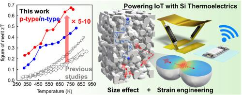
无线传感和传输设备的物联网的广泛应用需要由丰富且环保的材料组成的自供电模块。硅热电材料是一个很有前途的候选材料,并且已经以纳米级衍生物的形式实现了足够的性能值()。然而,将其扩大到散装材料,同时保持其稳定性一直具有挑战性。这种困难源于缺乏可扩展的纳米结构,既能有效地阻碍声子传输,又不会显著牺牲体过程中的电子传输,这是植根于电传输机制和热传输机制之间的内在权衡。为了克服这一限制,本研究通过高度非平衡烧结工艺引入了一种可扩展的3D软化纳米结构,其特点是纳米颗粒之间的传导路径狭窄,由于诱导的显著应变,有利于选择性的电子/声子界面传输。该应变工程的结果表明,n型和p型体三维硅纳米结构的应变值显著(室温下为0.11-0.23,750 K时为0.44-0.67),是先前报道的体纳米结构硅材料的5-10倍。优越的可扩展性使Si热电材料能够集成到灵活的模块中,并实现24小时为无线传感器设备供电。
本文章由计算机程序翻译,如有差异,请以英文原文为准。

Module-scale silicon 3D softened nanoarchitectures for eco-friendly thermoelectric energy harvesting

Module-scale silicon 3D softened nanoarchitectures for eco-friendly thermoelectric energy harvesting

Module-scale silicon 3D softened nanoarchitectures for eco-friendly thermoelectric energy harvesting
Widespread of internet-of-things with wireless sensing and transmission devices require self-powering module consisting of abundant and environmental-friendly materials. Si thermoelectric material is a promising candidate and sufficient figure of merit (zT) has been realized in the form of nanoscale derivatives. However, scaling it up to bulk material while maintaining the zT has been challenging. This difficulty arises from the lack of scalable nanostructures that effectively impede phonon transport without significantly sacrificing electron transport in the bulk process, which is rooted in the intrinsic trade-off between electrical and thermal transport mechanisms. To overcome this limitation, this study introduces a scalable 3D softened nanoarchitecture by a highly non-equilibrium sintering process, featuring narrow-conduction path between nanograins, which facilitates selective electron/phonon interface transmission due to the induced significant strain. This strain engineering results in remarkable zT values for both n- and p-type bulk 3D Si nanoarchitectures (0.11–0.23 at room temperature and 0.44–0.67 about 750 K), which are 5–10 times those of previously reported bulk nanostructured Si materials. The superior zT and scalability enables integrating the Si thermoelectric materials into a flexible module and realized powering wireless sensor devices for 24 h.
求助全文
通过发布文献求助,成功后即可免费获取论文全文。 去求助
来源期刊
Materials Today Physics
Materials Today Physics Materials Science-General Materials Science
CiteScore
14.00
自引率
7.80%
发文量
284
审稿时长
15 days
期刊介绍: Materials Today Physics is a multi-disciplinary journal focused on the physics of materials, encompassing both the physical properties and materials synthesis. Operating at the interface of physics and materials science, this journal covers one of the largest and most dynamic fields within physical science. The forefront research in materials physics is driving advancements in new materials, uncovering new physics, and fostering novel applications at an unprecedented pace.
×
引用
GB/T 7714-2015
复制
MLA
复制
APA
复制
导出至
BibTeX EndNote RefMan NoteFirst NoteExpress
×
提示
您的信息不完整,为了账户安全,请先补充。
现在去补充
×
提示
您因"违规操作"
具体请查看互助需知
我知道了
×
提示
确定
请完成安全验证×
copy
已复制链接
快去分享给好友吧!
我知道了
右上角分享
点击右上角分享
0
联系我们:info@booksci.cn Book学术提供免费学术资源搜索服务,方便国内外学者检索中英文文献。致力于提供最便捷和优质的服务体验。 Copyright © 2023 布克学术 All rights reserved.
京ICP备2023020795号-1
ghs 京公网安备 11010802042870号
Book学术文献互助
Book学术文献互助群
群 号:604180095
Book学术官方微信