Arash Ghobadi, Thomas B. Kallaos, Indeewari M. Karunarathne, Dilan M. Gamachchi, Andrew C. Meng, Joseph C. Mathai, Shubhra Gangopadhyay and Suchismita Guha
{"title":"聚合物铁电晶体管中的工程半导体-介电界面","authors":"Arash Ghobadi, Thomas B. Kallaos, Indeewari M. Karunarathne, Dilan M. Gamachchi, Andrew C. Meng, Joseph C. Mathai, Shubhra Gangopadhyay and Suchismita Guha","doi":"10.1039/D5TC01378J","DOIUrl":null,"url":null,"abstract":"<p >Polymer ferroelectrics are witnessing a renewed interest in organic transistors due to their multi-conductance states. Although their high dielectric constant allows low operating voltages, the polarization fluctuation due to the energetic disorder at the interface reduces the carrier mobility in organic transistors. Here, two copolymers of poly(vinylidene fluoride) (PVDF) with trifluoroethylene (TrFE) and hexafluoropropylene (HFP) as the dielectric layer, and a donor–acceptor copolymer as the active semiconductor layer are used in bottom-gate top-contact transistor architectures. We investigate the impact of the dielectric thickness, external poling, and an added interfacial ultrathin Al<small><sub>2</sub></small>O<small><sub>3</sub></small> layer at the semiconductor-dielectric surface on the performance of organic field-effect transistors (FETs). Although poling the dielectric layer significantly enhances the carrier mobility in PVDF-TrFE-based FETs, it has a minimal effect on PVDF-HFP-based devices. Poled PVDF-TrFE devices with a thickness of 45 nm show the highest saturation carrier mobility, exceeding 1 cm<small><sup>2</sup></small> V<small><sup>−1</sup></small> s<small><sup>−1</sup></small>. The subthreshold swing (SS), which is primarily governed by the trap states at the semiconductor–dielectric interface, is seen to significantly improve when an atomic layer deposited Al<small><sub>2</sub></small>O<small><sub>3</sub></small> film with varying thickness between 2 nm and 12 nm is deposited on PVDF-HFP. In the linear region of operation, PVDF-HFP based FETs with Al<small><sub>2</sub></small>O<small><sub>3</sub></small> yield SS values below 80 mV dec<small><sup>−1</sup></small>. The trap density of states at the semiconductor–dielectric interface was evaluated, providing deeper insight into charge trapping and transport mechanisms.</p>","PeriodicalId":84,"journal":{"name":"Journal of Materials Chemistry C","volume":" 26","pages":" 13454-13463"},"PeriodicalIF":5.1000,"publicationDate":"2025-05-30","publicationTypes":"Journal Article","fieldsOfStudy":null,"isOpenAccess":false,"openAccessPdf":"https://pubs.rsc.org/en/content/articlepdf/2025/tc/d5tc01378j?page=search","citationCount":"0","resultStr":"{\"title\":\"Engineered semiconductor-dielectric interfaces in polymer ferroelectric transistors†\",\"authors\":\"Arash Ghobadi, Thomas B. Kallaos, Indeewari M. Karunarathne, Dilan M. Gamachchi, Andrew C. Meng, Joseph C. Mathai, Shubhra Gangopadhyay and Suchismita Guha\",\"doi\":\"10.1039/D5TC01378J\",\"DOIUrl\":null,\"url\":null,\"abstract\":\"<p >Polymer ferroelectrics are witnessing a renewed interest in organic transistors due to their multi-conductance states. Although their high dielectric constant allows low operating voltages, the polarization fluctuation due to the energetic disorder at the interface reduces the carrier mobility in organic transistors. Here, two copolymers of poly(vinylidene fluoride) (PVDF) with trifluoroethylene (TrFE) and hexafluoropropylene (HFP) as the dielectric layer, and a donor–acceptor copolymer as the active semiconductor layer are used in bottom-gate top-contact transistor architectures. We investigate the impact of the dielectric thickness, external poling, and an added interfacial ultrathin Al<small><sub>2</sub></small>O<small><sub>3</sub></small> layer at the semiconductor-dielectric surface on the performance of organic field-effect transistors (FETs). Although poling the dielectric layer significantly enhances the carrier mobility in PVDF-TrFE-based FETs, it has a minimal effect on PVDF-HFP-based devices. Poled PVDF-TrFE devices with a thickness of 45 nm show the highest saturation carrier mobility, exceeding 1 cm<small><sup>2</sup></small> V<small><sup>−1</sup></small> s<small><sup>−1</sup></small>. The subthreshold swing (SS), which is primarily governed by the trap states at the semiconductor–dielectric interface, is seen to significantly improve when an atomic layer deposited Al<small><sub>2</sub></small>O<small><sub>3</sub></small> film with varying thickness between 2 nm and 12 nm is deposited on PVDF-HFP. In the linear region of operation, PVDF-HFP based FETs with Al<small><sub>2</sub></small>O<small><sub>3</sub></small> yield SS values below 80 mV dec<small><sup>−1</sup></small>. The trap density of states at the semiconductor–dielectric interface was evaluated, providing deeper insight into charge trapping and transport mechanisms.</p>\",\"PeriodicalId\":84,\"journal\":{\"name\":\"Journal of Materials Chemistry C\",\"volume\":\" 26\",\"pages\":\" 13454-13463\"},\"PeriodicalIF\":5.1000,\"publicationDate\":\"2025-05-30\",\"publicationTypes\":\"Journal Article\",\"fieldsOfStudy\":null,\"isOpenAccess\":false,\"openAccessPdf\":\"https://pubs.rsc.org/en/content/articlepdf/2025/tc/d5tc01378j?page=search\",\"citationCount\":\"0\",\"resultStr\":null,\"platform\":\"Semanticscholar\",\"paperid\":null,\"PeriodicalName\":\"Journal of Materials Chemistry C\",\"FirstCategoryId\":\"1\",\"ListUrlMain\":\"https://pubs.rsc.org/en/content/articlelanding/2025/tc/d5tc01378j\",\"RegionNum\":2,\"RegionCategory\":\"材料科学\",\"ArticlePicture\":[],\"TitleCN\":null,\"AbstractTextCN\":null,\"PMCID\":null,\"EPubDate\":\"\",\"PubModel\":\"\",\"JCR\":\"Q2\",\"JCRName\":\"MATERIALS SCIENCE, MULTIDISCIPLINARY\",\"Score\":null,\"Total\":0}","platform":"Semanticscholar","paperid":null,"PeriodicalName":"Journal of Materials Chemistry C","FirstCategoryId":"1","ListUrlMain":"https://pubs.rsc.org/en/content/articlelanding/2025/tc/d5tc01378j","RegionNum":2,"RegionCategory":"材料科学","ArticlePicture":[],"TitleCN":null,"AbstractTextCN":null,"PMCID":null,"EPubDate":"","PubModel":"","JCR":"Q2","JCRName":"MATERIALS SCIENCE, MULTIDISCIPLINARY","Score":null,"Total":0}
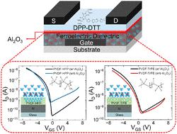
Engineered semiconductor-dielectric interfaces in polymer ferroelectric transistors†
Polymer ferroelectrics are witnessing a renewed interest in organic transistors due to their multi-conductance states. Although their high dielectric constant allows low operating voltages, the polarization fluctuation due to the energetic disorder at the interface reduces the carrier mobility in organic transistors. Here, two copolymers of poly(vinylidene fluoride) (PVDF) with trifluoroethylene (TrFE) and hexafluoropropylene (HFP) as the dielectric layer, and a donor–acceptor copolymer as the active semiconductor layer are used in bottom-gate top-contact transistor architectures. We investigate the impact of the dielectric thickness, external poling, and an added interfacial ultrathin Al2O3 layer at the semiconductor-dielectric surface on the performance of organic field-effect transistors (FETs). Although poling the dielectric layer significantly enhances the carrier mobility in PVDF-TrFE-based FETs, it has a minimal effect on PVDF-HFP-based devices. Poled PVDF-TrFE devices with a thickness of 45 nm show the highest saturation carrier mobility, exceeding 1 cm2 V−1 s−1. The subthreshold swing (SS), which is primarily governed by the trap states at the semiconductor–dielectric interface, is seen to significantly improve when an atomic layer deposited Al2O3 film with varying thickness between 2 nm and 12 nm is deposited on PVDF-HFP. In the linear region of operation, PVDF-HFP based FETs with Al2O3 yield SS values below 80 mV dec−1. The trap density of states at the semiconductor–dielectric interface was evaluated, providing deeper insight into charge trapping and transport mechanisms.
期刊介绍:
The Journal of Materials Chemistry is divided into three distinct sections, A, B, and C, each catering to specific applications of the materials under study:
Journal of Materials Chemistry A focuses primarily on materials intended for applications in energy and sustainability.
Journal of Materials Chemistry B specializes in materials designed for applications in biology and medicine.
Journal of Materials Chemistry C is dedicated to materials suitable for applications in optical, magnetic, and electronic devices.
Example topic areas within the scope of Journal of Materials Chemistry C are listed below. This list is neither exhaustive nor exclusive.
Bioelectronics
Conductors
Detectors
Dielectrics
Displays
Ferroelectrics
Lasers
LEDs
Lighting
Liquid crystals
Memory
Metamaterials
Multiferroics
Photonics
Photovoltaics
Semiconductors
Sensors
Single molecule conductors
Spintronics
Superconductors
Thermoelectrics
Topological insulators
Transistors

 求助内容:
求助内容: 应助结果提醒方式:


