Sepideh Faraji, Elke Meissner, Sven Besendörfer, Christian Miersch, Roland Weingärtner, Franziska C. Beyer, Jochen Friedrich
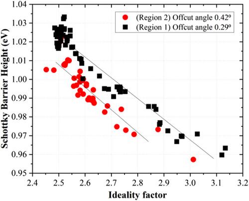
{"title":"氮化镓原生衬底非均匀边切角对氮化镓势垒层横向电流调制的影响","authors":"Sepideh Faraji, Elke Meissner, Sven Besendörfer, Christian Miersch, Roland Weingärtner, Franziska C. Beyer, Jochen Friedrich","doi":"10.1002/crat.202400245","DOIUrl":null,"url":null,"abstract":"<p>A comprehensive investigation on the uniformity of offcut angles on vicinal GaN substrate surfaces and their impact on both epitaxial growth and electrical characteristics of AlGaN/GaN heteroepitaxial structures is presented. A nearly inverse linear correlation is noted between the substrate's offcut angle and the Al mole fraction in the AlGaN layer. T During AlGaN growth, Ga atoms are obviously incorporated more to smaller atomic terraces as the Al atoms. Localized, non-uniform current conduction channels along the edges of bunched steps were observed. A larger substrate offcut results in higher occurrence of stripes with higher current flow. This affects the Schottky barrier height of diodes that contain different densities of such regions. Ni/Au/AlGaN/GaN Schottky barrier diodes showed a decrease in the average Schottky barrier height on such places. An offcut angle difference from 0.29° to 0.42° yields an approximately 13 meV reduction in average Schottky barrier height. This highlights the significant impact that the transition in surface morphology even at the initial stages could exert on the electrical characteristics of the Schottky barrier diodes. Consequently, it becomes crucial to accurately assess the offcut angle variations over the whole wafer to align epitaxy with the specific performance requirements of the target device.</p>","PeriodicalId":48935,"journal":{"name":"Crystal Research and Technology","volume":"60 6","pages":""},"PeriodicalIF":1.9000,"publicationDate":"2025-04-24","publicationTypes":"Journal Article","fieldsOfStudy":null,"isOpenAccess":false,"openAccessPdf":"https://onlinelibrary.wiley.com/doi/epdf/10.1002/crat.202400245","citationCount":"0","resultStr":"{\"title\":\"Impact of Inhomogeneous Offcut Angles of GaN Native Substrates on Lateral Current Modulation in AlGaN Barrier Layers\",\"authors\":\"Sepideh Faraji, Elke Meissner, Sven Besendörfer, Christian Miersch, Roland Weingärtner, Franziska C. Beyer, Jochen Friedrich\",\"doi\":\"10.1002/crat.202400245\",\"DOIUrl\":null,\"url\":null,\"abstract\":\"<p>A comprehensive investigation on the uniformity of offcut angles on vicinal GaN substrate surfaces and their impact on both epitaxial growth and electrical characteristics of AlGaN/GaN heteroepitaxial structures is presented. A nearly inverse linear correlation is noted between the substrate's offcut angle and the Al mole fraction in the AlGaN layer. T During AlGaN growth, Ga atoms are obviously incorporated more to smaller atomic terraces as the Al atoms. Localized, non-uniform current conduction channels along the edges of bunched steps were observed. A larger substrate offcut results in higher occurrence of stripes with higher current flow. This affects the Schottky barrier height of diodes that contain different densities of such regions. Ni/Au/AlGaN/GaN Schottky barrier diodes showed a decrease in the average Schottky barrier height on such places. An offcut angle difference from 0.29° to 0.42° yields an approximately 13 meV reduction in average Schottky barrier height. This highlights the significant impact that the transition in surface morphology even at the initial stages could exert on the electrical characteristics of the Schottky barrier diodes. Consequently, it becomes crucial to accurately assess the offcut angle variations over the whole wafer to align epitaxy with the specific performance requirements of the target device.</p>\",\"PeriodicalId\":48935,\"journal\":{\"name\":\"Crystal Research and Technology\",\"volume\":\"60 6\",\"pages\":\"\"},\"PeriodicalIF\":1.9000,\"publicationDate\":\"2025-04-24\",\"publicationTypes\":\"Journal Article\",\"fieldsOfStudy\":null,\"isOpenAccess\":false,\"openAccessPdf\":\"https://onlinelibrary.wiley.com/doi/epdf/10.1002/crat.202400245\",\"citationCount\":\"0\",\"resultStr\":null,\"platform\":\"Semanticscholar\",\"paperid\":null,\"PeriodicalName\":\"Crystal Research and Technology\",\"FirstCategoryId\":\"88\",\"ListUrlMain\":\"https://onlinelibrary.wiley.com/doi/10.1002/crat.202400245\",\"RegionNum\":4,\"RegionCategory\":\"材料科学\",\"ArticlePicture\":[],\"TitleCN\":null,\"AbstractTextCN\":null,\"PMCID\":null,\"EPubDate\":\"\",\"PubModel\":\"\",\"JCR\":\"Q3\",\"JCRName\":\"Chemistry\",\"Score\":null,\"Total\":0}","platform":"Semanticscholar","paperid":null,"PeriodicalName":"Crystal Research and Technology","FirstCategoryId":"88","ListUrlMain":"https://onlinelibrary.wiley.com/doi/10.1002/crat.202400245","RegionNum":4,"RegionCategory":"材料科学","ArticlePicture":[],"TitleCN":null,"AbstractTextCN":null,"PMCID":null,"EPubDate":"","PubModel":"","JCR":"Q3","JCRName":"Chemistry","Score":null,"Total":0}
Impact of Inhomogeneous Offcut Angles of GaN Native Substrates on Lateral Current Modulation in AlGaN Barrier Layers
A comprehensive investigation on the uniformity of offcut angles on vicinal GaN substrate surfaces and their impact on both epitaxial growth and electrical characteristics of AlGaN/GaN heteroepitaxial structures is presented. A nearly inverse linear correlation is noted between the substrate's offcut angle and the Al mole fraction in the AlGaN layer. T During AlGaN growth, Ga atoms are obviously incorporated more to smaller atomic terraces as the Al atoms. Localized, non-uniform current conduction channels along the edges of bunched steps were observed. A larger substrate offcut results in higher occurrence of stripes with higher current flow. This affects the Schottky barrier height of diodes that contain different densities of such regions. Ni/Au/AlGaN/GaN Schottky barrier diodes showed a decrease in the average Schottky barrier height on such places. An offcut angle difference from 0.29° to 0.42° yields an approximately 13 meV reduction in average Schottky barrier height. This highlights the significant impact that the transition in surface morphology even at the initial stages could exert on the electrical characteristics of the Schottky barrier diodes. Consequently, it becomes crucial to accurately assess the offcut angle variations over the whole wafer to align epitaxy with the specific performance requirements of the target device.
期刊介绍:
The journal Crystal Research and Technology is a pure online Journal (since 2012).
Crystal Research and Technology is an international journal examining all aspects of research within experimental, industrial, and theoretical crystallography. The journal covers the relevant aspects of
-crystal growth techniques and phenomena (including bulk growth, thin films)
-modern crystalline materials (e.g. smart materials, nanocrystals, quasicrystals, liquid crystals)
-industrial crystallisation
-application of crystals in materials science, electronics, data storage, and optics
-experimental, simulation and theoretical studies of the structural properties of crystals
-crystallographic computing
 求助内容:
求助内容: 应助结果提醒方式:


