Santanu Kandar, Kamlesh Bhatt, Shivansh Tiwari, Nahid Chaudhary, Taslim Khan, Ashok Kapoor and Rajendra Singh
{"title":"用于高速可见光-近红外光探测的MoSe2/GaTe范德华异质结构的可扩展MBE生长","authors":"Santanu Kandar, Kamlesh Bhatt, Shivansh Tiwari, Nahid Chaudhary, Taslim Khan, Ashok Kapoor and Rajendra Singh","doi":"10.1039/D5TC00645G","DOIUrl":null,"url":null,"abstract":"<p >Two-dimensional (2D) material-based photodetectors have gained significant attention in recent years due to their ultrafast response times and tunable optoelectronic properties. As the demand for photodetectors with enhanced responsivity across different wavelengths increases, 2D/2D heterostructures have become a key focus for overcoming the limitations of traditional metal–semiconductor–metal (MSM) photodetectors. In this work, we report a high-performance visible-near-infrared (NIR) photodetector based on a MoSe<small><sub>2</sub></small>/GaTe heterostructure grown using a molecular beam epitaxy (MBE) system on a SiO<small><sub>2</sub></small>/Si substrate. The heterostructure exhibits a type-III (broken-gap) band alignment, facilitating efficient charge separation and enabling higher responsivity across ultraviolet (UV), visible, and NIR wavelengths compared to the MSM-GaTe-based device. The photodetector achieves the highest responsivity of 0.6 A W<small><sup>−1</sup></small> at 200 nm in the UV region while demonstrating fast response times of 44 ms (rise) and 67 ms (decay) under 780 nm visible illumination. In the NIR range (1000 nm), response times extend to 242 ms (rise) and 340 ms (decay), maintaining strong photodetection capability. The transient current spikes observed under 780 nm illumination arise from the pyroelectric effect, attributed to GaTe's non-centrosymmetric nature, highlighting the interplay of thermal and photoelectric contributions. This unique combination of features makes the MoSe<small><sub>2</sub></small>/GaTe heterostructure an attractive candidate for advanced photodetection applications in the visible and NIR wavelength ranges.</p>","PeriodicalId":84,"journal":{"name":"Journal of Materials Chemistry C","volume":" 21","pages":" 10529-10541"},"PeriodicalIF":5.1000,"publicationDate":"2025-05-13","publicationTypes":"Journal Article","fieldsOfStudy":null,"isOpenAccess":false,"openAccessPdf":"","citationCount":"0","resultStr":"{\"title\":\"Scalable MBE growth of MoSe2/GaTe van der Waals heterostructure for high-speed vis-NIR photodetection†\",\"authors\":\"Santanu Kandar, Kamlesh Bhatt, Shivansh Tiwari, Nahid Chaudhary, Taslim Khan, Ashok Kapoor and Rajendra Singh\",\"doi\":\"10.1039/D5TC00645G\",\"DOIUrl\":null,\"url\":null,\"abstract\":\"<p >Two-dimensional (2D) material-based photodetectors have gained significant attention in recent years due to their ultrafast response times and tunable optoelectronic properties. As the demand for photodetectors with enhanced responsivity across different wavelengths increases, 2D/2D heterostructures have become a key focus for overcoming the limitations of traditional metal–semiconductor–metal (MSM) photodetectors. In this work, we report a high-performance visible-near-infrared (NIR) photodetector based on a MoSe<small><sub>2</sub></small>/GaTe heterostructure grown using a molecular beam epitaxy (MBE) system on a SiO<small><sub>2</sub></small>/Si substrate. The heterostructure exhibits a type-III (broken-gap) band alignment, facilitating efficient charge separation and enabling higher responsivity across ultraviolet (UV), visible, and NIR wavelengths compared to the MSM-GaTe-based device. The photodetector achieves the highest responsivity of 0.6 A W<small><sup>−1</sup></small> at 200 nm in the UV region while demonstrating fast response times of 44 ms (rise) and 67 ms (decay) under 780 nm visible illumination. In the NIR range (1000 nm), response times extend to 242 ms (rise) and 340 ms (decay), maintaining strong photodetection capability. The transient current spikes observed under 780 nm illumination arise from the pyroelectric effect, attributed to GaTe's non-centrosymmetric nature, highlighting the interplay of thermal and photoelectric contributions. This unique combination of features makes the MoSe<small><sub>2</sub></small>/GaTe heterostructure an attractive candidate for advanced photodetection applications in the visible and NIR wavelength ranges.</p>\",\"PeriodicalId\":84,\"journal\":{\"name\":\"Journal of Materials Chemistry C\",\"volume\":\" 21\",\"pages\":\" 10529-10541\"},\"PeriodicalIF\":5.1000,\"publicationDate\":\"2025-05-13\",\"publicationTypes\":\"Journal Article\",\"fieldsOfStudy\":null,\"isOpenAccess\":false,\"openAccessPdf\":\"\",\"citationCount\":\"0\",\"resultStr\":null,\"platform\":\"Semanticscholar\",\"paperid\":null,\"PeriodicalName\":\"Journal of Materials Chemistry C\",\"FirstCategoryId\":\"1\",\"ListUrlMain\":\"https://pubs.rsc.org/en/content/articlelanding/2025/tc/d5tc00645g\",\"RegionNum\":2,\"RegionCategory\":\"材料科学\",\"ArticlePicture\":[],\"TitleCN\":null,\"AbstractTextCN\":null,\"PMCID\":null,\"EPubDate\":\"\",\"PubModel\":\"\",\"JCR\":\"Q2\",\"JCRName\":\"MATERIALS SCIENCE, MULTIDISCIPLINARY\",\"Score\":null,\"Total\":0}","platform":"Semanticscholar","paperid":null,"PeriodicalName":"Journal of Materials Chemistry C","FirstCategoryId":"1","ListUrlMain":"https://pubs.rsc.org/en/content/articlelanding/2025/tc/d5tc00645g","RegionNum":2,"RegionCategory":"材料科学","ArticlePicture":[],"TitleCN":null,"AbstractTextCN":null,"PMCID":null,"EPubDate":"","PubModel":"","JCR":"Q2","JCRName":"MATERIALS SCIENCE, MULTIDISCIPLINARY","Score":null,"Total":0}
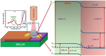
Scalable MBE growth of MoSe2/GaTe van der Waals heterostructure for high-speed vis-NIR photodetection†
Two-dimensional (2D) material-based photodetectors have gained significant attention in recent years due to their ultrafast response times and tunable optoelectronic properties. As the demand for photodetectors with enhanced responsivity across different wavelengths increases, 2D/2D heterostructures have become a key focus for overcoming the limitations of traditional metal–semiconductor–metal (MSM) photodetectors. In this work, we report a high-performance visible-near-infrared (NIR) photodetector based on a MoSe2/GaTe heterostructure grown using a molecular beam epitaxy (MBE) system on a SiO2/Si substrate. The heterostructure exhibits a type-III (broken-gap) band alignment, facilitating efficient charge separation and enabling higher responsivity across ultraviolet (UV), visible, and NIR wavelengths compared to the MSM-GaTe-based device. The photodetector achieves the highest responsivity of 0.6 A W−1 at 200 nm in the UV region while demonstrating fast response times of 44 ms (rise) and 67 ms (decay) under 780 nm visible illumination. In the NIR range (1000 nm), response times extend to 242 ms (rise) and 340 ms (decay), maintaining strong photodetection capability. The transient current spikes observed under 780 nm illumination arise from the pyroelectric effect, attributed to GaTe's non-centrosymmetric nature, highlighting the interplay of thermal and photoelectric contributions. This unique combination of features makes the MoSe2/GaTe heterostructure an attractive candidate for advanced photodetection applications in the visible and NIR wavelength ranges.
期刊介绍:
The Journal of Materials Chemistry is divided into three distinct sections, A, B, and C, each catering to specific applications of the materials under study:
Journal of Materials Chemistry A focuses primarily on materials intended for applications in energy and sustainability.
Journal of Materials Chemistry B specializes in materials designed for applications in biology and medicine.
Journal of Materials Chemistry C is dedicated to materials suitable for applications in optical, magnetic, and electronic devices.
Example topic areas within the scope of Journal of Materials Chemistry C are listed below. This list is neither exhaustive nor exclusive.
Bioelectronics
Conductors
Detectors
Dielectrics
Displays
Ferroelectrics
Lasers
LEDs
Lighting
Liquid crystals
Memory
Metamaterials
Multiferroics
Photonics
Photovoltaics
Semiconductors
Sensors
Single molecule conductors
Spintronics
Superconductors
Thermoelectrics
Topological insulators
Transistors

 求助内容:
求助内容: 应助结果提醒方式:


