Jun Wang, Xin-Wang Yao, Xiu-Xing Xu, Xia Wu, Jun-Han Qian, Xiu-Juan Wang, Yan-Fang Liu, Chun-Yan Wu and Lin-Bao Luo
{"title":"SnO/β-Ga2O3异质结势垒肖特基二极管降低反向漏电流和提高击穿电压†","authors":"Jun Wang, Xin-Wang Yao, Xiu-Xing Xu, Xia Wu, Jun-Han Qian, Xiu-Juan Wang, Yan-Fang Liu, Chun-Yan Wu and Lin-Bao Luo","doi":"10.1039/D5TC01355K","DOIUrl":null,"url":null,"abstract":"<p >In this article, we report a vertical β-Ga<small><sub>2</sub></small>O<small><sub>3</sub></small> heterojunction barrier Schottky (HJBS) diode fabricated by using reactive magnetron sputtering to selectively grow a circular p-type SnO film array. Compared to its Schottky barrier diode (SBD) counterpart, the HJBS diode shows a slightly increased turn-on voltage (<em>V</em><small><sub>on</sub></small>) and specific on-resistance (<em>R</em><small><sub>on,sp</sub></small>), but its breakdown voltage (BV) is greatly improved due to the decreased electric field crowding effect at the anode edge as well as the lateral surface depletion effect of the SnO/β-Ga<small><sub>2</sub></small>O<small><sub>3</sub></small> p–n junction. A BV of 1375 V and a Baliga's power figure of merit (PFOM) of 0.37 GW cm<small><sup>−2</sup></small> achieved for the device with a spacing of 3 μm are expected to be improved by further shrinking the spacing. Meanwhile, the reverse leakage current (<em>J</em><small><sub>R</sub></small>) is lower than 2 μA cm<small><sup>−2</sup></small> (the detection limit of the system) even at a reverse bias (<em>V</em><small><sub>R</sub></small>) of 1250 V. The SnO/β-Ga<small><sub>2</sub></small>O<small><sub>3</sub></small> HJBS diodes show great promise for use in future β-Ga<small><sub>2</sub></small>O<small><sub>3</sub></small> power electronic devices with high PFOM, while maintaining a suppressed reverse leakage current.</p>","PeriodicalId":84,"journal":{"name":"Journal of Materials Chemistry C","volume":" 20","pages":" 9992-9996"},"PeriodicalIF":5.1000,"publicationDate":"2025-04-28","publicationTypes":"Journal Article","fieldsOfStudy":null,"isOpenAccess":false,"openAccessPdf":"","citationCount":"0","resultStr":"{\"title\":\"SnO/β-Ga2O3 heterojunction barrier Schottky diodes for decreased reverse leakage current and improved breakdown voltage†\",\"authors\":\"Jun Wang, Xin-Wang Yao, Xiu-Xing Xu, Xia Wu, Jun-Han Qian, Xiu-Juan Wang, Yan-Fang Liu, Chun-Yan Wu and Lin-Bao Luo\",\"doi\":\"10.1039/D5TC01355K\",\"DOIUrl\":null,\"url\":null,\"abstract\":\"<p >In this article, we report a vertical β-Ga<small><sub>2</sub></small>O<small><sub>3</sub></small> heterojunction barrier Schottky (HJBS) diode fabricated by using reactive magnetron sputtering to selectively grow a circular p-type SnO film array. Compared to its Schottky barrier diode (SBD) counterpart, the HJBS diode shows a slightly increased turn-on voltage (<em>V</em><small><sub>on</sub></small>) and specific on-resistance (<em>R</em><small><sub>on,sp</sub></small>), but its breakdown voltage (BV) is greatly improved due to the decreased electric field crowding effect at the anode edge as well as the lateral surface depletion effect of the SnO/β-Ga<small><sub>2</sub></small>O<small><sub>3</sub></small> p–n junction. A BV of 1375 V and a Baliga's power figure of merit (PFOM) of 0.37 GW cm<small><sup>−2</sup></small> achieved for the device with a spacing of 3 μm are expected to be improved by further shrinking the spacing. Meanwhile, the reverse leakage current (<em>J</em><small><sub>R</sub></small>) is lower than 2 μA cm<small><sup>−2</sup></small> (the detection limit of the system) even at a reverse bias (<em>V</em><small><sub>R</sub></small>) of 1250 V. The SnO/β-Ga<small><sub>2</sub></small>O<small><sub>3</sub></small> HJBS diodes show great promise for use in future β-Ga<small><sub>2</sub></small>O<small><sub>3</sub></small> power electronic devices with high PFOM, while maintaining a suppressed reverse leakage current.</p>\",\"PeriodicalId\":84,\"journal\":{\"name\":\"Journal of Materials Chemistry C\",\"volume\":\" 20\",\"pages\":\" 9992-9996\"},\"PeriodicalIF\":5.1000,\"publicationDate\":\"2025-04-28\",\"publicationTypes\":\"Journal Article\",\"fieldsOfStudy\":null,\"isOpenAccess\":false,\"openAccessPdf\":\"\",\"citationCount\":\"0\",\"resultStr\":null,\"platform\":\"Semanticscholar\",\"paperid\":null,\"PeriodicalName\":\"Journal of Materials Chemistry C\",\"FirstCategoryId\":\"1\",\"ListUrlMain\":\"https://pubs.rsc.org/en/content/articlelanding/2025/tc/d5tc01355k\",\"RegionNum\":2,\"RegionCategory\":\"材料科学\",\"ArticlePicture\":[],\"TitleCN\":null,\"AbstractTextCN\":null,\"PMCID\":null,\"EPubDate\":\"\",\"PubModel\":\"\",\"JCR\":\"Q2\",\"JCRName\":\"MATERIALS SCIENCE, MULTIDISCIPLINARY\",\"Score\":null,\"Total\":0}","platform":"Semanticscholar","paperid":null,"PeriodicalName":"Journal of Materials Chemistry C","FirstCategoryId":"1","ListUrlMain":"https://pubs.rsc.org/en/content/articlelanding/2025/tc/d5tc01355k","RegionNum":2,"RegionCategory":"材料科学","ArticlePicture":[],"TitleCN":null,"AbstractTextCN":null,"PMCID":null,"EPubDate":"","PubModel":"","JCR":"Q2","JCRName":"MATERIALS SCIENCE, MULTIDISCIPLINARY","Score":null,"Total":0}
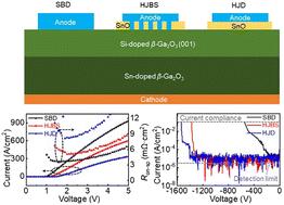
SnO/β-Ga2O3 heterojunction barrier Schottky diodes for decreased reverse leakage current and improved breakdown voltage†
In this article, we report a vertical β-Ga2O3 heterojunction barrier Schottky (HJBS) diode fabricated by using reactive magnetron sputtering to selectively grow a circular p-type SnO film array. Compared to its Schottky barrier diode (SBD) counterpart, the HJBS diode shows a slightly increased turn-on voltage (Von) and specific on-resistance (Ron,sp), but its breakdown voltage (BV) is greatly improved due to the decreased electric field crowding effect at the anode edge as well as the lateral surface depletion effect of the SnO/β-Ga2O3 p–n junction. A BV of 1375 V and a Baliga's power figure of merit (PFOM) of 0.37 GW cm−2 achieved for the device with a spacing of 3 μm are expected to be improved by further shrinking the spacing. Meanwhile, the reverse leakage current (JR) is lower than 2 μA cm−2 (the detection limit of the system) even at a reverse bias (VR) of 1250 V. The SnO/β-Ga2O3 HJBS diodes show great promise for use in future β-Ga2O3 power electronic devices with high PFOM, while maintaining a suppressed reverse leakage current.
期刊介绍:
The Journal of Materials Chemistry is divided into three distinct sections, A, B, and C, each catering to specific applications of the materials under study:
Journal of Materials Chemistry A focuses primarily on materials intended for applications in energy and sustainability.
Journal of Materials Chemistry B specializes in materials designed for applications in biology and medicine.
Journal of Materials Chemistry C is dedicated to materials suitable for applications in optical, magnetic, and electronic devices.
Example topic areas within the scope of Journal of Materials Chemistry C are listed below. This list is neither exhaustive nor exclusive.
Bioelectronics
Conductors
Detectors
Dielectrics
Displays
Ferroelectrics
Lasers
LEDs
Lighting
Liquid crystals
Memory
Metamaterials
Multiferroics
Photonics
Photovoltaics
Semiconductors
Sensors
Single molecule conductors
Spintronics
Superconductors
Thermoelectrics
Topological insulators
Transistors

 求助内容:
求助内容: 应助结果提醒方式:


