Xingyu Zhang, Min Guo, Jia Li, Tingting Dai, Zihong Yang, Zhidong Lou, Yanbing Hou, Feng Teng and Yufeng Hu
{"title":"低压钙钛矿发光晶体管:利用溶液处理的高k无机电介质进行全彩发射的新方法","authors":"Xingyu Zhang, Min Guo, Jia Li, Tingting Dai, Zihong Yang, Zhidong Lou, Yanbing Hou, Feng Teng and Yufeng Hu","doi":"10.1039/D5TC00231A","DOIUrl":null,"url":null,"abstract":"<p >Perovskite materials have garnered significant attention in recent years due to their exceptional optoelectronic properties, making them promising candidates for a wide range of electroluminescent applications. Among these, perovskite light-emitting transistors (PeLETs), which integrate perovskite-based light-emitting layers, have been extensively studied. However, a key challenge remains: most reported PeLETs require high operating voltages ranging from tens to hundreds of volts, limiting their practical use in applications such as active-matrix displays. In this study, we introduce a high-<em>k</em> dielectric layer of HfO<small><sub><em>x</em></sub></small> in the fabrication of perovskite thin-film light-emitting transistors, achieving a significant reduction in operating voltage. The device, employing an optimized structure, operates at a low source–drain voltage of just 4 V. To further enhance device performance, PEA<small><sup>+</sup></small> cations are incorporated to modify CsPbI<small><sub>3</sub></small>/Br<small><sub>3</sub></small>, and by adjusting the halogen composition, red, green, and blue PeLETs are realized. The maximum mobility values for the red, green, and blue devices are 0.74 cm<small><sup>2</sup></small> V<small><sup>−1</sup></small> s<small><sup>−1</sup></small>, 0.67 cm<small><sup>2</sup></small> V<small><sup>−1</sup></small> s<small><sup>−1</sup></small>, and 0.66 cm<small><sup>2</sup></small> V<small><sup>−1</sup></small> s<small><sup>−1</sup></small>, respectively. Notably, we report the first-ever blue-emitting perovskite thin-film light-emitting transistor, providing critical insights into the low-voltage operation of PeLETs and their potential for application in future full-color display technologies.</p>","PeriodicalId":84,"journal":{"name":"Journal of Materials Chemistry C","volume":" 17","pages":" 8694-8701"},"PeriodicalIF":5.1000,"publicationDate":"2025-03-19","publicationTypes":"Journal Article","fieldsOfStudy":null,"isOpenAccess":false,"openAccessPdf":"","citationCount":"0","resultStr":"{\"title\":\"Low-voltage perovskite light-emitting transistors: a novel approach utilizing solution-processed high-k inorganic dielectrics for full-color emission†\",\"authors\":\"Xingyu Zhang, Min Guo, Jia Li, Tingting Dai, Zihong Yang, Zhidong Lou, Yanbing Hou, Feng Teng and Yufeng Hu\",\"doi\":\"10.1039/D5TC00231A\",\"DOIUrl\":null,\"url\":null,\"abstract\":\"<p >Perovskite materials have garnered significant attention in recent years due to their exceptional optoelectronic properties, making them promising candidates for a wide range of electroluminescent applications. Among these, perovskite light-emitting transistors (PeLETs), which integrate perovskite-based light-emitting layers, have been extensively studied. However, a key challenge remains: most reported PeLETs require high operating voltages ranging from tens to hundreds of volts, limiting their practical use in applications such as active-matrix displays. In this study, we introduce a high-<em>k</em> dielectric layer of HfO<small><sub><em>x</em></sub></small> in the fabrication of perovskite thin-film light-emitting transistors, achieving a significant reduction in operating voltage. The device, employing an optimized structure, operates at a low source–drain voltage of just 4 V. To further enhance device performance, PEA<small><sup>+</sup></small> cations are incorporated to modify CsPbI<small><sub>3</sub></small>/Br<small><sub>3</sub></small>, and by adjusting the halogen composition, red, green, and blue PeLETs are realized. The maximum mobility values for the red, green, and blue devices are 0.74 cm<small><sup>2</sup></small> V<small><sup>−1</sup></small> s<small><sup>−1</sup></small>, 0.67 cm<small><sup>2</sup></small> V<small><sup>−1</sup></small> s<small><sup>−1</sup></small>, and 0.66 cm<small><sup>2</sup></small> V<small><sup>−1</sup></small> s<small><sup>−1</sup></small>, respectively. Notably, we report the first-ever blue-emitting perovskite thin-film light-emitting transistor, providing critical insights into the low-voltage operation of PeLETs and their potential for application in future full-color display technologies.</p>\",\"PeriodicalId\":84,\"journal\":{\"name\":\"Journal of Materials Chemistry C\",\"volume\":\" 17\",\"pages\":\" 8694-8701\"},\"PeriodicalIF\":5.1000,\"publicationDate\":\"2025-03-19\",\"publicationTypes\":\"Journal Article\",\"fieldsOfStudy\":null,\"isOpenAccess\":false,\"openAccessPdf\":\"\",\"citationCount\":\"0\",\"resultStr\":null,\"platform\":\"Semanticscholar\",\"paperid\":null,\"PeriodicalName\":\"Journal of Materials Chemistry C\",\"FirstCategoryId\":\"1\",\"ListUrlMain\":\"https://pubs.rsc.org/en/content/articlelanding/2025/tc/d5tc00231a\",\"RegionNum\":2,\"RegionCategory\":\"材料科学\",\"ArticlePicture\":[],\"TitleCN\":null,\"AbstractTextCN\":null,\"PMCID\":null,\"EPubDate\":\"\",\"PubModel\":\"\",\"JCR\":\"Q2\",\"JCRName\":\"MATERIALS SCIENCE, MULTIDISCIPLINARY\",\"Score\":null,\"Total\":0}","platform":"Semanticscholar","paperid":null,"PeriodicalName":"Journal of Materials Chemistry C","FirstCategoryId":"1","ListUrlMain":"https://pubs.rsc.org/en/content/articlelanding/2025/tc/d5tc00231a","RegionNum":2,"RegionCategory":"材料科学","ArticlePicture":[],"TitleCN":null,"AbstractTextCN":null,"PMCID":null,"EPubDate":"","PubModel":"","JCR":"Q2","JCRName":"MATERIALS SCIENCE, MULTIDISCIPLINARY","Score":null,"Total":0}
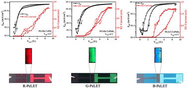
Low-voltage perovskite light-emitting transistors: a novel approach utilizing solution-processed high-k inorganic dielectrics for full-color emission†
Perovskite materials have garnered significant attention in recent years due to their exceptional optoelectronic properties, making them promising candidates for a wide range of electroluminescent applications. Among these, perovskite light-emitting transistors (PeLETs), which integrate perovskite-based light-emitting layers, have been extensively studied. However, a key challenge remains: most reported PeLETs require high operating voltages ranging from tens to hundreds of volts, limiting their practical use in applications such as active-matrix displays. In this study, we introduce a high-k dielectric layer of HfOx in the fabrication of perovskite thin-film light-emitting transistors, achieving a significant reduction in operating voltage. The device, employing an optimized structure, operates at a low source–drain voltage of just 4 V. To further enhance device performance, PEA+ cations are incorporated to modify CsPbI3/Br3, and by adjusting the halogen composition, red, green, and blue PeLETs are realized. The maximum mobility values for the red, green, and blue devices are 0.74 cm2 V−1 s−1, 0.67 cm2 V−1 s−1, and 0.66 cm2 V−1 s−1, respectively. Notably, we report the first-ever blue-emitting perovskite thin-film light-emitting transistor, providing critical insights into the low-voltage operation of PeLETs and their potential for application in future full-color display technologies.
期刊介绍:
The Journal of Materials Chemistry is divided into three distinct sections, A, B, and C, each catering to specific applications of the materials under study:
Journal of Materials Chemistry A focuses primarily on materials intended for applications in energy and sustainability.
Journal of Materials Chemistry B specializes in materials designed for applications in biology and medicine.
Journal of Materials Chemistry C is dedicated to materials suitable for applications in optical, magnetic, and electronic devices.
Example topic areas within the scope of Journal of Materials Chemistry C are listed below. This list is neither exhaustive nor exclusive.
Bioelectronics
Conductors
Detectors
Dielectrics
Displays
Ferroelectrics
Lasers
LEDs
Lighting
Liquid crystals
Memory
Metamaterials
Multiferroics
Photonics
Photovoltaics
Semiconductors
Sensors
Single molecule conductors
Spintronics
Superconductors
Thermoelectrics
Topological insulators
Transistors

 求助内容:
求助内容: 应助结果提醒方式:


