{"title":"胶体二维ZnO纳米片溶液法制备低压TFT及其在紫外光电探测器上的应用","authors":"Abhik Bhuin, Akhilesh Kumar Yadav, Utkarsh Pandey, Debdyuti Mukherjee, Vivek Kumar Agrahari, Caroline Ponraj, Subha Sadhu, Bhola Nath Pal and Sujoy Sarkar","doi":"10.1039/D4TC05180G","DOIUrl":null,"url":null,"abstract":"<p >ZnO nanostructures have been extensively employed in optoelectronic devices because of their unique optoelectronic properties; however, these devices have been developed using physical vapor deposition techniques, which are costly and need a state-of-the-art fabrication facility. Hence, a solution-processed, cost-effective, low-temperature method is required for the large-scale fabrication of 2D material-based electronic devices. In this contribution, we report template, polymer, and surfactant-free wet chemical synthesis of 2D ZnO nanostructures having dimensions of ∼200 nm and thickness of ∼30 nm following the hydrothermal method. Detailed structural, morphological, and optical investigation revealed the formation of a pure hexagonal wurtzite phase of ZnO nanosheets. Utilizing the as-synthesized nanosheets, solution-processed thin film transistors (TFTs) are fabricated under low annealing temperatures that exhibit a high carrier mobility of 8.05 cm<small><sup>2</sup></small> V<small><sup>−1</sup></small> s<small><sup>−1</sup></small> and an on–off ratio of ∼10<small><sup>5</sup></small>. Also, these TFTs show high photosensitivity and can be used as UV detectors. Thus, our study highlights low-temperature facile fabrication of 2D ZnO TFTs, which may have promising applications in electronic displays, logic circuits, UV detectors, biosensors, and portable electronics.</p>","PeriodicalId":84,"journal":{"name":"Journal of Materials Chemistry C","volume":" 17","pages":" 8763-8775"},"PeriodicalIF":5.1000,"publicationDate":"2025-03-17","publicationTypes":"Journal Article","fieldsOfStudy":null,"isOpenAccess":false,"openAccessPdf":"","citationCount":"0","resultStr":"{\"title\":\"Fabrication of a solution-processed low voltage TFT by using colloid 2D ZnO nanosheets and its application as a UV photodetector†\",\"authors\":\"Abhik Bhuin, Akhilesh Kumar Yadav, Utkarsh Pandey, Debdyuti Mukherjee, Vivek Kumar Agrahari, Caroline Ponraj, Subha Sadhu, Bhola Nath Pal and Sujoy Sarkar\",\"doi\":\"10.1039/D4TC05180G\",\"DOIUrl\":null,\"url\":null,\"abstract\":\"<p >ZnO nanostructures have been extensively employed in optoelectronic devices because of their unique optoelectronic properties; however, these devices have been developed using physical vapor deposition techniques, which are costly and need a state-of-the-art fabrication facility. Hence, a solution-processed, cost-effective, low-temperature method is required for the large-scale fabrication of 2D material-based electronic devices. In this contribution, we report template, polymer, and surfactant-free wet chemical synthesis of 2D ZnO nanostructures having dimensions of ∼200 nm and thickness of ∼30 nm following the hydrothermal method. Detailed structural, morphological, and optical investigation revealed the formation of a pure hexagonal wurtzite phase of ZnO nanosheets. Utilizing the as-synthesized nanosheets, solution-processed thin film transistors (TFTs) are fabricated under low annealing temperatures that exhibit a high carrier mobility of 8.05 cm<small><sup>2</sup></small> V<small><sup>−1</sup></small> s<small><sup>−1</sup></small> and an on–off ratio of ∼10<small><sup>5</sup></small>. Also, these TFTs show high photosensitivity and can be used as UV detectors. Thus, our study highlights low-temperature facile fabrication of 2D ZnO TFTs, which may have promising applications in electronic displays, logic circuits, UV detectors, biosensors, and portable electronics.</p>\",\"PeriodicalId\":84,\"journal\":{\"name\":\"Journal of Materials Chemistry C\",\"volume\":\" 17\",\"pages\":\" 8763-8775\"},\"PeriodicalIF\":5.1000,\"publicationDate\":\"2025-03-17\",\"publicationTypes\":\"Journal Article\",\"fieldsOfStudy\":null,\"isOpenAccess\":false,\"openAccessPdf\":\"\",\"citationCount\":\"0\",\"resultStr\":null,\"platform\":\"Semanticscholar\",\"paperid\":null,\"PeriodicalName\":\"Journal of Materials Chemistry C\",\"FirstCategoryId\":\"1\",\"ListUrlMain\":\"https://pubs.rsc.org/en/content/articlelanding/2025/tc/d4tc05180g\",\"RegionNum\":2,\"RegionCategory\":\"材料科学\",\"ArticlePicture\":[],\"TitleCN\":null,\"AbstractTextCN\":null,\"PMCID\":null,\"EPubDate\":\"\",\"PubModel\":\"\",\"JCR\":\"Q2\",\"JCRName\":\"MATERIALS SCIENCE, MULTIDISCIPLINARY\",\"Score\":null,\"Total\":0}","platform":"Semanticscholar","paperid":null,"PeriodicalName":"Journal of Materials Chemistry C","FirstCategoryId":"1","ListUrlMain":"https://pubs.rsc.org/en/content/articlelanding/2025/tc/d4tc05180g","RegionNum":2,"RegionCategory":"材料科学","ArticlePicture":[],"TitleCN":null,"AbstractTextCN":null,"PMCID":null,"EPubDate":"","PubModel":"","JCR":"Q2","JCRName":"MATERIALS SCIENCE, MULTIDISCIPLINARY","Score":null,"Total":0}
Fabrication of a solution-processed low voltage TFT by using colloid 2D ZnO nanosheets and its application as a UV photodetector†
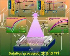
ZnO nanostructures have been extensively employed in optoelectronic devices because of their unique optoelectronic properties; however, these devices have been developed using physical vapor deposition techniques, which are costly and need a state-of-the-art fabrication facility. Hence, a solution-processed, cost-effective, low-temperature method is required for the large-scale fabrication of 2D material-based electronic devices. In this contribution, we report template, polymer, and surfactant-free wet chemical synthesis of 2D ZnO nanostructures having dimensions of ∼200 nm and thickness of ∼30 nm following the hydrothermal method. Detailed structural, morphological, and optical investigation revealed the formation of a pure hexagonal wurtzite phase of ZnO nanosheets. Utilizing the as-synthesized nanosheets, solution-processed thin film transistors (TFTs) are fabricated under low annealing temperatures that exhibit a high carrier mobility of 8.05 cm2 V−1 s−1 and an on–off ratio of ∼105. Also, these TFTs show high photosensitivity and can be used as UV detectors. Thus, our study highlights low-temperature facile fabrication of 2D ZnO TFTs, which may have promising applications in electronic displays, logic circuits, UV detectors, biosensors, and portable electronics.
期刊介绍:
The Journal of Materials Chemistry is divided into three distinct sections, A, B, and C, each catering to specific applications of the materials under study:
Journal of Materials Chemistry A focuses primarily on materials intended for applications in energy and sustainability.
Journal of Materials Chemistry B specializes in materials designed for applications in biology and medicine.
Journal of Materials Chemistry C is dedicated to materials suitable for applications in optical, magnetic, and electronic devices.
Example topic areas within the scope of Journal of Materials Chemistry C are listed below. This list is neither exhaustive nor exclusive.
Bioelectronics
Conductors
Detectors
Dielectrics
Displays
Ferroelectrics
Lasers
LEDs
Lighting
Liquid crystals
Memory
Metamaterials
Multiferroics
Photonics
Photovoltaics
Semiconductors
Sensors
Single molecule conductors
Spintronics
Superconductors
Thermoelectrics
Topological insulators
Transistors

 求助内容:
求助内容: 应助结果提醒方式:


