Kiyung Kim, Minjae Kim, Yongsu Lee, Hae-Won Lee, Jae Hyeon Jun, Jun-Hyeok Choi, Seongbeen Yoon, Hyeon-Jun Hwang, Byoung Hun Lee
{"title":"垂直堆叠ZnO/Te互补场效应晶体管的演示","authors":"Kiyung Kim, Minjae Kim, Yongsu Lee, Hae-Won Lee, Jae Hyeon Jun, Jun-Hyeok Choi, Seongbeen Yoon, Hyeon-Jun Hwang, Byoung Hun Lee","doi":"10.1002/aelm.202500031","DOIUrl":null,"url":null,"abstract":"<p>The complementary field-effect transistor (CFET) structure is a highly area-efficient technology. However, their fabrication entails highly complex integration processes using wafer transfer or recrystallization, which has been limiting further development. In this paper, an alternative method is proposed to realize CFETs using p-type tellurium (Te) (for the lower-level channel) and n-type zinc oxide (ZnO) (for the upper-level channel). Te and ZnO are directly deposited on a 30 × 30 mm<sup>2</sup> SiO<sub>2</sub>/Silicon substrate, using a considerably low-temperature fabrication process (<150 °C). The lower p-type channel exhibits superior mobility exceeding 10 cm<sup>2</sup> V<sup>−1</sup> s<sup>−1</sup> even after the integration of the entire CFET process. The CFET inverter demonstrates a voltage gain >51 at <i>V</i><sub>DD</sub> = 4 V and noise margins of 0.36 and 0.45 V at <i>V</i><sub>DD</sub> = 1 V. Using the same integration process, functional NAND and NOR logic gates are successfully demonstrated in the vertically integrated CFET structure. The proposed ZnO/Te CFET can be a promising device technology, particularly for 3D and heterojunction integration requiring a low thermal budget.</p>","PeriodicalId":110,"journal":{"name":"Advanced Electronic Materials","volume":"11 12","pages":""},"PeriodicalIF":5.3000,"publicationDate":"2025-04-03","publicationTypes":"Journal Article","fieldsOfStudy":null,"isOpenAccess":false,"openAccessPdf":"https://onlinelibrary.wiley.com/doi/epdf/10.1002/aelm.202500031","citationCount":"0","resultStr":"{\"title\":\"Demonstration of Vertically Stacked ZnO/Te Complementary Field-Effect Transistor\",\"authors\":\"Kiyung Kim, Minjae Kim, Yongsu Lee, Hae-Won Lee, Jae Hyeon Jun, Jun-Hyeok Choi, Seongbeen Yoon, Hyeon-Jun Hwang, Byoung Hun Lee\",\"doi\":\"10.1002/aelm.202500031\",\"DOIUrl\":null,\"url\":null,\"abstract\":\"<p>The complementary field-effect transistor (CFET) structure is a highly area-efficient technology. However, their fabrication entails highly complex integration processes using wafer transfer or recrystallization, which has been limiting further development. In this paper, an alternative method is proposed to realize CFETs using p-type tellurium (Te) (for the lower-level channel) and n-type zinc oxide (ZnO) (for the upper-level channel). Te and ZnO are directly deposited on a 30 × 30 mm<sup>2</sup> SiO<sub>2</sub>/Silicon substrate, using a considerably low-temperature fabrication process (<150 °C). The lower p-type channel exhibits superior mobility exceeding 10 cm<sup>2</sup> V<sup>−1</sup> s<sup>−1</sup> even after the integration of the entire CFET process. The CFET inverter demonstrates a voltage gain >51 at <i>V</i><sub>DD</sub> = 4 V and noise margins of 0.36 and 0.45 V at <i>V</i><sub>DD</sub> = 1 V. Using the same integration process, functional NAND and NOR logic gates are successfully demonstrated in the vertically integrated CFET structure. The proposed ZnO/Te CFET can be a promising device technology, particularly for 3D and heterojunction integration requiring a low thermal budget.</p>\",\"PeriodicalId\":110,\"journal\":{\"name\":\"Advanced Electronic Materials\",\"volume\":\"11 12\",\"pages\":\"\"},\"PeriodicalIF\":5.3000,\"publicationDate\":\"2025-04-03\",\"publicationTypes\":\"Journal Article\",\"fieldsOfStudy\":null,\"isOpenAccess\":false,\"openAccessPdf\":\"https://onlinelibrary.wiley.com/doi/epdf/10.1002/aelm.202500031\",\"citationCount\":\"0\",\"resultStr\":null,\"platform\":\"Semanticscholar\",\"paperid\":null,\"PeriodicalName\":\"Advanced Electronic Materials\",\"FirstCategoryId\":\"88\",\"ListUrlMain\":\"https://advanced.onlinelibrary.wiley.com/doi/10.1002/aelm.202500031\",\"RegionNum\":2,\"RegionCategory\":\"材料科学\",\"ArticlePicture\":[],\"TitleCN\":null,\"AbstractTextCN\":null,\"PMCID\":null,\"EPubDate\":\"\",\"PubModel\":\"\",\"JCR\":\"Q2\",\"JCRName\":\"MATERIALS SCIENCE, MULTIDISCIPLINARY\",\"Score\":null,\"Total\":0}","platform":"Semanticscholar","paperid":null,"PeriodicalName":"Advanced Electronic Materials","FirstCategoryId":"88","ListUrlMain":"https://advanced.onlinelibrary.wiley.com/doi/10.1002/aelm.202500031","RegionNum":2,"RegionCategory":"材料科学","ArticlePicture":[],"TitleCN":null,"AbstractTextCN":null,"PMCID":null,"EPubDate":"","PubModel":"","JCR":"Q2","JCRName":"MATERIALS SCIENCE, MULTIDISCIPLINARY","Score":null,"Total":0}
Demonstration of Vertically Stacked ZnO/Te Complementary Field-Effect Transistor
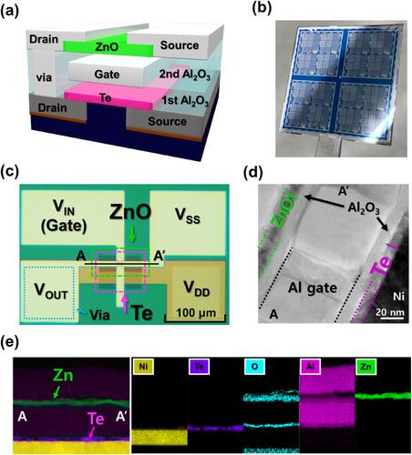
The complementary field-effect transistor (CFET) structure is a highly area-efficient technology. However, their fabrication entails highly complex integration processes using wafer transfer or recrystallization, which has been limiting further development. In this paper, an alternative method is proposed to realize CFETs using p-type tellurium (Te) (for the lower-level channel) and n-type zinc oxide (ZnO) (for the upper-level channel). Te and ZnO are directly deposited on a 30 × 30 mm2 SiO2/Silicon substrate, using a considerably low-temperature fabrication process (<150 °C). The lower p-type channel exhibits superior mobility exceeding 10 cm2 V−1 s−1 even after the integration of the entire CFET process. The CFET inverter demonstrates a voltage gain >51 at VDD = 4 V and noise margins of 0.36 and 0.45 V at VDD = 1 V. Using the same integration process, functional NAND and NOR logic gates are successfully demonstrated in the vertically integrated CFET structure. The proposed ZnO/Te CFET can be a promising device technology, particularly for 3D and heterojunction integration requiring a low thermal budget.
期刊介绍:
Advanced Electronic Materials is an interdisciplinary forum for peer-reviewed, high-quality, high-impact research in the fields of materials science, physics, and engineering of electronic and magnetic materials. It includes research on physics and physical properties of electronic and magnetic materials, spintronics, electronics, device physics and engineering, micro- and nano-electromechanical systems, and organic electronics, in addition to fundamental research.


 求助内容:
求助内容: 应助结果提醒方式:


