Mohammad Masum Billah, Md Mobaidul Islam, Sunaina Priyadarshi, Jung Bae Kim, Yang Ho Bae, Rodney Lim, Dejiu Fan, Zero Hung, Dong Kil Yim, Soo Yong Choi, Youron Lin, Juergen Grillmayer, Custer Ma, Lynn Yang, Julian Chen, Jin Jang
{"title":"多通道非晶氧化物薄膜晶体管具有 67 cm2 V-1 s-1 的高迁移率和出色的稳定性","authors":"Mohammad Masum Billah, Md Mobaidul Islam, Sunaina Priyadarshi, Jung Bae Kim, Yang Ho Bae, Rodney Lim, Dejiu Fan, Zero Hung, Dong Kil Yim, Soo Yong Choi, Youron Lin, Juergen Grillmayer, Custer Ma, Lynn Yang, Julian Chen, Jin Jang","doi":"10.1002/aelm.202400766","DOIUrl":null,"url":null,"abstract":"<p>Multi-channel amorphous oxide thin-film transistors (TFTs) with dual gate (DG), coplanar structure are studied. The multi-channel consists of a top amorphous indium gallium zinc tin oxide (a-IGZTO) and a very thin amorphous indium zinc oxide (a-IZO) bottom layer. The fabricated TFTs exhibit high field-effect mobility (µ<sub>FE</sub>) ≈67.1 cm<sup>2</sup> V<sup>−1</sup> s<sup>−1</sup>, and excellent stability under positive bias temperature stress (PBTS). The band diagram of the multi-channel TFT is presented based on UV photoelectron spectroscopy, X-ray photoelectron spectroscopy, and UV–vis spectroscopy measurements. The PBTS robustness is interpreted as the formation of 2D electron gas (2DEG) at the a-IGZTO/a-IZO hetero-interface which extends to the bulk a-IZO layer. From thermalization energy (E<sub>Th</sub>) analysis with the energy barrier to defect formation under PBTS, the multi-channel TFT exhibits the largest E<sub>Th</sub> of 0.84 eV, which indicates that more stress energy is needed for threshold voltage shift during PBTS in the TFTs as compared to single-channel TFTs.</p>","PeriodicalId":110,"journal":{"name":"Advanced Electronic Materials","volume":"11 8","pages":""},"PeriodicalIF":5.3000,"publicationDate":"2025-03-30","publicationTypes":"Journal Article","fieldsOfStudy":null,"isOpenAccess":false,"openAccessPdf":"https://onlinelibrary.wiley.com/doi/epdf/10.1002/aelm.202400766","citationCount":"0","resultStr":"{\"title\":\"Multi-Channel, Amorphous Oxide Thin-Film Transistor Exhibiting High Mobility of 67 cm2 V−1 s−1 and Excellent Stability\",\"authors\":\"Mohammad Masum Billah, Md Mobaidul Islam, Sunaina Priyadarshi, Jung Bae Kim, Yang Ho Bae, Rodney Lim, Dejiu Fan, Zero Hung, Dong Kil Yim, Soo Yong Choi, Youron Lin, Juergen Grillmayer, Custer Ma, Lynn Yang, Julian Chen, Jin Jang\",\"doi\":\"10.1002/aelm.202400766\",\"DOIUrl\":null,\"url\":null,\"abstract\":\"<p>Multi-channel amorphous oxide thin-film transistors (TFTs) with dual gate (DG), coplanar structure are studied. The multi-channel consists of a top amorphous indium gallium zinc tin oxide (a-IGZTO) and a very thin amorphous indium zinc oxide (a-IZO) bottom layer. The fabricated TFTs exhibit high field-effect mobility (µ<sub>FE</sub>) ≈67.1 cm<sup>2</sup> V<sup>−1</sup> s<sup>−1</sup>, and excellent stability under positive bias temperature stress (PBTS). The band diagram of the multi-channel TFT is presented based on UV photoelectron spectroscopy, X-ray photoelectron spectroscopy, and UV–vis spectroscopy measurements. The PBTS robustness is interpreted as the formation of 2D electron gas (2DEG) at the a-IGZTO/a-IZO hetero-interface which extends to the bulk a-IZO layer. From thermalization energy (E<sub>Th</sub>) analysis with the energy barrier to defect formation under PBTS, the multi-channel TFT exhibits the largest E<sub>Th</sub> of 0.84 eV, which indicates that more stress energy is needed for threshold voltage shift during PBTS in the TFTs as compared to single-channel TFTs.</p>\",\"PeriodicalId\":110,\"journal\":{\"name\":\"Advanced Electronic Materials\",\"volume\":\"11 8\",\"pages\":\"\"},\"PeriodicalIF\":5.3000,\"publicationDate\":\"2025-03-30\",\"publicationTypes\":\"Journal Article\",\"fieldsOfStudy\":null,\"isOpenAccess\":false,\"openAccessPdf\":\"https://onlinelibrary.wiley.com/doi/epdf/10.1002/aelm.202400766\",\"citationCount\":\"0\",\"resultStr\":null,\"platform\":\"Semanticscholar\",\"paperid\":null,\"PeriodicalName\":\"Advanced Electronic Materials\",\"FirstCategoryId\":\"88\",\"ListUrlMain\":\"https://advanced.onlinelibrary.wiley.com/doi/10.1002/aelm.202400766\",\"RegionNum\":2,\"RegionCategory\":\"材料科学\",\"ArticlePicture\":[],\"TitleCN\":null,\"AbstractTextCN\":null,\"PMCID\":null,\"EPubDate\":\"\",\"PubModel\":\"\",\"JCR\":\"Q2\",\"JCRName\":\"MATERIALS SCIENCE, MULTIDISCIPLINARY\",\"Score\":null,\"Total\":0}","platform":"Semanticscholar","paperid":null,"PeriodicalName":"Advanced Electronic Materials","FirstCategoryId":"88","ListUrlMain":"https://advanced.onlinelibrary.wiley.com/doi/10.1002/aelm.202400766","RegionNum":2,"RegionCategory":"材料科学","ArticlePicture":[],"TitleCN":null,"AbstractTextCN":null,"PMCID":null,"EPubDate":"","PubModel":"","JCR":"Q2","JCRName":"MATERIALS SCIENCE, MULTIDISCIPLINARY","Score":null,"Total":0}
Multi-Channel, Amorphous Oxide Thin-Film Transistor Exhibiting High Mobility of 67 cm2 V−1 s−1 and Excellent Stability
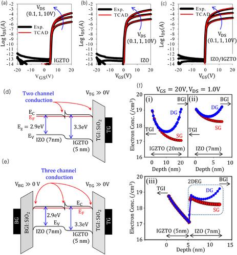
Multi-channel amorphous oxide thin-film transistors (TFTs) with dual gate (DG), coplanar structure are studied. The multi-channel consists of a top amorphous indium gallium zinc tin oxide (a-IGZTO) and a very thin amorphous indium zinc oxide (a-IZO) bottom layer. The fabricated TFTs exhibit high field-effect mobility (µFE) ≈67.1 cm2 V−1 s−1, and excellent stability under positive bias temperature stress (PBTS). The band diagram of the multi-channel TFT is presented based on UV photoelectron spectroscopy, X-ray photoelectron spectroscopy, and UV–vis spectroscopy measurements. The PBTS robustness is interpreted as the formation of 2D electron gas (2DEG) at the a-IGZTO/a-IZO hetero-interface which extends to the bulk a-IZO layer. From thermalization energy (ETh) analysis with the energy barrier to defect formation under PBTS, the multi-channel TFT exhibits the largest ETh of 0.84 eV, which indicates that more stress energy is needed for threshold voltage shift during PBTS in the TFTs as compared to single-channel TFTs.
期刊介绍:
Advanced Electronic Materials is an interdisciplinary forum for peer-reviewed, high-quality, high-impact research in the fields of materials science, physics, and engineering of electronic and magnetic materials. It includes research on physics and physical properties of electronic and magnetic materials, spintronics, electronics, device physics and engineering, micro- and nano-electromechanical systems, and organic electronics, in addition to fundamental research.


 求助内容:
求助内容: 应助结果提醒方式:


