Hui Wang, Peishan Li, Zexin Dong, Yuqing Yang, Huan Chang, Chenguang He, Qiao Wang, Zhitao Chen, Kang Zhang and Xingfu Wang
{"title":"低温直接键合制备的硅基InGaN/GaN微带蓝色发光二极管","authors":"Hui Wang, Peishan Li, Zexin Dong, Yuqing Yang, Huan Chang, Chenguang He, Qiao Wang, Zhitao Chen, Kang Zhang and Xingfu Wang","doi":"10.1039/D4TC03237C","DOIUrl":null,"url":null,"abstract":"<p >Integrating a nitride semiconductor light source on Si is a key to building wide-spectrum photonic systems; however, there have been many challenges in growing nitride semiconductors directly on a Si substrate. Herein, freestanding InGaN/GaN-based microbelts were first prepared by using the electrochemical lift-off (ELO) technique from an as-grown sapphire substrate. The obtained microbelts had uniform morphology and could be flexibly transferred. Subsequently, direct bonding technology was used to transfer and integrate the released InGaN/GaN-based microbelt onto a high conductivity Si substrate to fabricate an on-chip microbelt light-emitting diode (MBLED) with a vertical injection structure. An intermediate amorphous layer with a thickness of ∼25 nm was formed at the interface of GaN and Si, which was found to have no obvious negative effect on the electrical injection of the MBLED. The prepared Si-based InGaN/GaN MBLED emitted a 465 nm light at the end face of the microbelt with unidirectional luminescent waveguide properties. The luminescence intensity showed a high linear correlation with increasing current. Fowler–Nordheim tunneling (FNT) and thermionic emission (TE) were found to be responsible for its current transport mechanisms at low and high voltages, respectively. This study provides a simple, low-cost method for integrating III–V semiconductor devices on a Si substrate.</p>","PeriodicalId":84,"journal":{"name":"Journal of Materials Chemistry C","volume":" 7","pages":" 3283-3291"},"PeriodicalIF":5.1000,"publicationDate":"2024-12-16","publicationTypes":"Journal Article","fieldsOfStudy":null,"isOpenAccess":false,"openAccessPdf":"","citationCount":"0","resultStr":"{\"title\":\"A silicon-based InGaN/GaN microbelt blue light-emitting-diode fabricated via low-temperature direct bonding\",\"authors\":\"Hui Wang, Peishan Li, Zexin Dong, Yuqing Yang, Huan Chang, Chenguang He, Qiao Wang, Zhitao Chen, Kang Zhang and Xingfu Wang\",\"doi\":\"10.1039/D4TC03237C\",\"DOIUrl\":null,\"url\":null,\"abstract\":\"<p >Integrating a nitride semiconductor light source on Si is a key to building wide-spectrum photonic systems; however, there have been many challenges in growing nitride semiconductors directly on a Si substrate. Herein, freestanding InGaN/GaN-based microbelts were first prepared by using the electrochemical lift-off (ELO) technique from an as-grown sapphire substrate. The obtained microbelts had uniform morphology and could be flexibly transferred. Subsequently, direct bonding technology was used to transfer and integrate the released InGaN/GaN-based microbelt onto a high conductivity Si substrate to fabricate an on-chip microbelt light-emitting diode (MBLED) with a vertical injection structure. An intermediate amorphous layer with a thickness of ∼25 nm was formed at the interface of GaN and Si, which was found to have no obvious negative effect on the electrical injection of the MBLED. The prepared Si-based InGaN/GaN MBLED emitted a 465 nm light at the end face of the microbelt with unidirectional luminescent waveguide properties. The luminescence intensity showed a high linear correlation with increasing current. Fowler–Nordheim tunneling (FNT) and thermionic emission (TE) were found to be responsible for its current transport mechanisms at low and high voltages, respectively. This study provides a simple, low-cost method for integrating III–V semiconductor devices on a Si substrate.</p>\",\"PeriodicalId\":84,\"journal\":{\"name\":\"Journal of Materials Chemistry C\",\"volume\":\" 7\",\"pages\":\" 3283-3291\"},\"PeriodicalIF\":5.1000,\"publicationDate\":\"2024-12-16\",\"publicationTypes\":\"Journal Article\",\"fieldsOfStudy\":null,\"isOpenAccess\":false,\"openAccessPdf\":\"\",\"citationCount\":\"0\",\"resultStr\":null,\"platform\":\"Semanticscholar\",\"paperid\":null,\"PeriodicalName\":\"Journal of Materials Chemistry C\",\"FirstCategoryId\":\"1\",\"ListUrlMain\":\"https://pubs.rsc.org/en/content/articlelanding/2025/tc/d4tc03237c\",\"RegionNum\":2,\"RegionCategory\":\"材料科学\",\"ArticlePicture\":[],\"TitleCN\":null,\"AbstractTextCN\":null,\"PMCID\":null,\"EPubDate\":\"\",\"PubModel\":\"\",\"JCR\":\"Q2\",\"JCRName\":\"MATERIALS SCIENCE, MULTIDISCIPLINARY\",\"Score\":null,\"Total\":0}","platform":"Semanticscholar","paperid":null,"PeriodicalName":"Journal of Materials Chemistry C","FirstCategoryId":"1","ListUrlMain":"https://pubs.rsc.org/en/content/articlelanding/2025/tc/d4tc03237c","RegionNum":2,"RegionCategory":"材料科学","ArticlePicture":[],"TitleCN":null,"AbstractTextCN":null,"PMCID":null,"EPubDate":"","PubModel":"","JCR":"Q2","JCRName":"MATERIALS SCIENCE, MULTIDISCIPLINARY","Score":null,"Total":0}
A silicon-based InGaN/GaN microbelt blue light-emitting-diode fabricated via low-temperature direct bonding
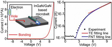
Integrating a nitride semiconductor light source on Si is a key to building wide-spectrum photonic systems; however, there have been many challenges in growing nitride semiconductors directly on a Si substrate. Herein, freestanding InGaN/GaN-based microbelts were first prepared by using the electrochemical lift-off (ELO) technique from an as-grown sapphire substrate. The obtained microbelts had uniform morphology and could be flexibly transferred. Subsequently, direct bonding technology was used to transfer and integrate the released InGaN/GaN-based microbelt onto a high conductivity Si substrate to fabricate an on-chip microbelt light-emitting diode (MBLED) with a vertical injection structure. An intermediate amorphous layer with a thickness of ∼25 nm was formed at the interface of GaN and Si, which was found to have no obvious negative effect on the electrical injection of the MBLED. The prepared Si-based InGaN/GaN MBLED emitted a 465 nm light at the end face of the microbelt with unidirectional luminescent waveguide properties. The luminescence intensity showed a high linear correlation with increasing current. Fowler–Nordheim tunneling (FNT) and thermionic emission (TE) were found to be responsible for its current transport mechanisms at low and high voltages, respectively. This study provides a simple, low-cost method for integrating III–V semiconductor devices on a Si substrate.
期刊介绍:
The Journal of Materials Chemistry is divided into three distinct sections, A, B, and C, each catering to specific applications of the materials under study:
Journal of Materials Chemistry A focuses primarily on materials intended for applications in energy and sustainability.
Journal of Materials Chemistry B specializes in materials designed for applications in biology and medicine.
Journal of Materials Chemistry C is dedicated to materials suitable for applications in optical, magnetic, and electronic devices.
Example topic areas within the scope of Journal of Materials Chemistry C are listed below. This list is neither exhaustive nor exclusive.
Bioelectronics
Conductors
Detectors
Dielectrics
Displays
Ferroelectrics
Lasers
LEDs
Lighting
Liquid crystals
Memory
Metamaterials
Multiferroics
Photonics
Photovoltaics
Semiconductors
Sensors
Single molecule conductors
Spintronics
Superconductors
Thermoelectrics
Topological insulators
Transistors

 求助内容:
求助内容: 应助结果提醒方式:


