{"title":"低暗电流、高探测率的Cu2O/Ga2O3 pn结光电探测器","authors":"Mingyang Li, Dayong Jiang and Man Zhao","doi":"10.1039/D4TC04165H","DOIUrl":null,"url":null,"abstract":"<p >Cu<small><sub>2</sub></small>O is a natural p-type semiconductor material with a high optical absorption coefficient in the visible range. It possesses characteristics such as abundant raw materials, low cost, non-toxicity, no pollution, and high theoretical photoelectric conversion efficiency. At present, achieving p-type doping in Ga<small><sub>2</sub></small>O<small><sub>3</sub></small> is challenging, making the preparation of Ga<small><sub>2</sub></small>O<small><sub>3</sub></small> homojunction photodetectors a significant recent challenge. Combining n-Ga<small><sub>2</sub></small>O<small><sub>3</sub></small> with p-type semiconductors to prepare pn heterojunction photodetectors offers an effective alternative approach. Based on this, this article combines electrochemically grown Cu<small><sub>2</sub></small>O with magnetron sputtered amorphous Ga<small><sub>2</sub></small>O<small><sub>3</sub></small> to prepare a low dark current and high detectivity Cu<small><sub>2</sub></small>O/Ga<small><sub>2</sub></small>O<small><sub>3</sub></small> ultraviolet visible heterojunction photodetector. The photodetector exhibits a low dark current of 1.58 × 10<small><sup>−9</sup></small> A and a high rectification ratio of 10<small><sup>3</sup></small> under a −5 V bias. It shows a peak responsivity of 4.26 A W<small><sup>−1</sup></small> and an EQE of 977.91% at a wavelength of 540 nm. Additionally, the photodetector has a detectivity of 1.17 × 10<small><sup>12</sup></small> Jones, an NEP of 4.80 × 10<small><sup>−13</sup></small> W Hz<small><sup>−1/2</sup></small>, and rise and fall times of 0.49 and 0.70 s, respectively. Comparing it with Cu<small><sub>2</sub></small>O PD, it is demonstrated that the reason for the improvement of the photodetector is due to the built-in electric field formed by the heterojunction, which can effectively separate electron hole pairs and suppress their recombination. This work provides a simple and effective method for preparing Cu<small><sub>2</sub></small>O heterojunction photodetectors.</p>","PeriodicalId":84,"journal":{"name":"Journal of Materials Chemistry C","volume":" 2","pages":" 718-723"},"PeriodicalIF":5.1000,"publicationDate":"2024-11-04","publicationTypes":"Journal Article","fieldsOfStudy":null,"isOpenAccess":false,"openAccessPdf":"","citationCount":"0","resultStr":"{\"title\":\"Cu2O/Ga2O3 pn-junction photodetector with low dark current and high detectivity\",\"authors\":\"Mingyang Li, Dayong Jiang and Man Zhao\",\"doi\":\"10.1039/D4TC04165H\",\"DOIUrl\":null,\"url\":null,\"abstract\":\"<p >Cu<small><sub>2</sub></small>O is a natural p-type semiconductor material with a high optical absorption coefficient in the visible range. It possesses characteristics such as abundant raw materials, low cost, non-toxicity, no pollution, and high theoretical photoelectric conversion efficiency. At present, achieving p-type doping in Ga<small><sub>2</sub></small>O<small><sub>3</sub></small> is challenging, making the preparation of Ga<small><sub>2</sub></small>O<small><sub>3</sub></small> homojunction photodetectors a significant recent challenge. Combining n-Ga<small><sub>2</sub></small>O<small><sub>3</sub></small> with p-type semiconductors to prepare pn heterojunction photodetectors offers an effective alternative approach. Based on this, this article combines electrochemically grown Cu<small><sub>2</sub></small>O with magnetron sputtered amorphous Ga<small><sub>2</sub></small>O<small><sub>3</sub></small> to prepare a low dark current and high detectivity Cu<small><sub>2</sub></small>O/Ga<small><sub>2</sub></small>O<small><sub>3</sub></small> ultraviolet visible heterojunction photodetector. The photodetector exhibits a low dark current of 1.58 × 10<small><sup>−9</sup></small> A and a high rectification ratio of 10<small><sup>3</sup></small> under a −5 V bias. It shows a peak responsivity of 4.26 A W<small><sup>−1</sup></small> and an EQE of 977.91% at a wavelength of 540 nm. Additionally, the photodetector has a detectivity of 1.17 × 10<small><sup>12</sup></small> Jones, an NEP of 4.80 × 10<small><sup>−13</sup></small> W Hz<small><sup>−1/2</sup></small>, and rise and fall times of 0.49 and 0.70 s, respectively. Comparing it with Cu<small><sub>2</sub></small>O PD, it is demonstrated that the reason for the improvement of the photodetector is due to the built-in electric field formed by the heterojunction, which can effectively separate electron hole pairs and suppress their recombination. This work provides a simple and effective method for preparing Cu<small><sub>2</sub></small>O heterojunction photodetectors.</p>\",\"PeriodicalId\":84,\"journal\":{\"name\":\"Journal of Materials Chemistry C\",\"volume\":\" 2\",\"pages\":\" 718-723\"},\"PeriodicalIF\":5.1000,\"publicationDate\":\"2024-11-04\",\"publicationTypes\":\"Journal Article\",\"fieldsOfStudy\":null,\"isOpenAccess\":false,\"openAccessPdf\":\"\",\"citationCount\":\"0\",\"resultStr\":null,\"platform\":\"Semanticscholar\",\"paperid\":null,\"PeriodicalName\":\"Journal of Materials Chemistry C\",\"FirstCategoryId\":\"1\",\"ListUrlMain\":\"https://pubs.rsc.org/en/content/articlelanding/2025/tc/d4tc04165h\",\"RegionNum\":2,\"RegionCategory\":\"材料科学\",\"ArticlePicture\":[],\"TitleCN\":null,\"AbstractTextCN\":null,\"PMCID\":null,\"EPubDate\":\"\",\"PubModel\":\"\",\"JCR\":\"Q2\",\"JCRName\":\"MATERIALS SCIENCE, MULTIDISCIPLINARY\",\"Score\":null,\"Total\":0}","platform":"Semanticscholar","paperid":null,"PeriodicalName":"Journal of Materials Chemistry C","FirstCategoryId":"1","ListUrlMain":"https://pubs.rsc.org/en/content/articlelanding/2025/tc/d4tc04165h","RegionNum":2,"RegionCategory":"材料科学","ArticlePicture":[],"TitleCN":null,"AbstractTextCN":null,"PMCID":null,"EPubDate":"","PubModel":"","JCR":"Q2","JCRName":"MATERIALS SCIENCE, MULTIDISCIPLINARY","Score":null,"Total":0}
引用次数: 0
摘要
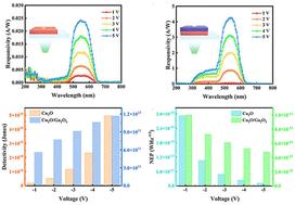
Cu2O是一种天然的p型半导体材料,在可见光范围内具有较高的光吸收系数。它具有原料丰富、成本低、无毒、无污染、理论光电转换效率高等特点。目前,在Ga2O3中实现p型掺杂是具有挑战性的,这使得制备Ga2O3同质结光电探测器成为最近的一个重大挑战。结合n-Ga2O3与p型半导体制备pn异质结光电探测器提供了一种有效的替代方法。在此基础上,本文将电化学生长的Cu2O与磁控溅射的非晶Ga2O3相结合,制备了低暗电流、高探测率的Cu2O/Ga2O3紫外可见异质结光电探测器。该光电探测器在−5 V偏置下具有1.58 × 10⁻⁹ a的低暗电流和103的高整流比。在540nm波长处,其峰值响应度为4.26 a W−1,EQE为977.91%。此外,光电探测器的探测率为1.17 × 10¹² Jones, NEP为4.80 × 10⁻¹³ W Hz−1/2,上升和下降时间分别为0.49和0.70 s。将其与Cu2O PD进行比较,证明光电探测器性能提高的原因是由于异质结形成的内置电场,可以有效地分离电子空穴对并抑制它们的复合。本工作为制备Cu2O异质结光电探测器提供了一种简单有效的方法。
Cu2O/Ga2O3 pn-junction photodetector with low dark current and high detectivity
Cu2O is a natural p-type semiconductor material with a high optical absorption coefficient in the visible range. It possesses characteristics such as abundant raw materials, low cost, non-toxicity, no pollution, and high theoretical photoelectric conversion efficiency. At present, achieving p-type doping in Ga2O3 is challenging, making the preparation of Ga2O3 homojunction photodetectors a significant recent challenge. Combining n-Ga2O3 with p-type semiconductors to prepare pn heterojunction photodetectors offers an effective alternative approach. Based on this, this article combines electrochemically grown Cu2O with magnetron sputtered amorphous Ga2O3 to prepare a low dark current and high detectivity Cu2O/Ga2O3 ultraviolet visible heterojunction photodetector. The photodetector exhibits a low dark current of 1.58 × 10⁻⁹ A and a high rectification ratio of 103 under a −5 V bias. It shows a peak responsivity of 4.26 A W−1 and an EQE of 977.91% at a wavelength of 540 nm. Additionally, the photodetector has a detectivity of 1.17 × 10¹² Jones, an NEP of 4.80 × 10⁻¹³ W Hz−1/2, and rise and fall times of 0.49 and 0.70 s, respectively. Comparing it with Cu2O PD, it is demonstrated that the reason for the improvement of the photodetector is due to the built-in electric field formed by the heterojunction, which can effectively separate electron hole pairs and suppress their recombination. This work provides a simple and effective method for preparing Cu2O heterojunction photodetectors.
期刊介绍:
The Journal of Materials Chemistry is divided into three distinct sections, A, B, and C, each catering to specific applications of the materials under study:
Journal of Materials Chemistry A focuses primarily on materials intended for applications in energy and sustainability.
Journal of Materials Chemistry B specializes in materials designed for applications in biology and medicine.
Journal of Materials Chemistry C is dedicated to materials suitable for applications in optical, magnetic, and electronic devices.
Example topic areas within the scope of Journal of Materials Chemistry C are listed below. This list is neither exhaustive nor exclusive.
Bioelectronics
Conductors
Detectors
Dielectrics
Displays
Ferroelectrics
Lasers
LEDs
Lighting
Liquid crystals
Memory
Metamaterials
Multiferroics
Photonics
Photovoltaics
Semiconductors
Sensors
Single molecule conductors
Spintronics
Superconductors
Thermoelectrics
Topological insulators
Transistors

 求助内容:
求助内容: 应助结果提醒方式:


