Andrea Pulici, Stefano Kuschlan, Gabriele Seguini, Marco De Michielis, Riccardo Chiarcos, Michele Laus, Marco Fanciulli and Michele Perego
{"title":"掺杂磷端端聚合物的超薄硅-绝缘体薄膜中的供体不完全电离和迁移率增强","authors":"Andrea Pulici, Stefano Kuschlan, Gabriele Seguini, Marco De Michielis, Riccardo Chiarcos, Michele Laus, Marco Fanciulli and Michele Perego","doi":"10.1039/D4TC01886A","DOIUrl":null,"url":null,"abstract":"<p >\r\n <em>Ex situ</em> doping of ultra-thin silicon-on-insulator (SOI) substrates is performed by using polymers terminated with a doping containing moiety. The injection of P impurity atoms is investigated confining the same P dose of ∼ 1 × 10<small><sup>13</sup></small> cm<small><sup>−2</sup></small> in a progressively thinner device layer, with thickness values (<em>H</em><small><sub>SOI</sub></small>) from 6 to 70 nm. The dopant concentration is determined by Time-of-flight secondary ion mass spectroscopy (ToF-SIMS) measurements. Sample resistivity (<em>ρ</em>), carrier concentration (<em>n</em><small><sub>e</sub></small>) and mobility (<em>μ</em>) are determined combining sheet resistance and Hall measurements in van der Pauw configuration. Almost complete activation and full ionization of the injected dopants is observed at room temperature in the samples with <em>H</em><small><sub>SOI</sub></small> ≥ 30 nm. The ionization fraction progressively drops to 5% when reducing the thickness of the device layer. Dopant incomplete ionization is accompanied by an increase in electron mobility, with values significantly larger than those reported for bulk Si. In the SOI samples with <em>H</em><small><sub>SOI</sub></small> > 20 nm, the fraction of ionized P atoms at room temperature is perfectly described by the 3D bulk model of Altermatt <em>et al.</em> For <em>H</em><small><sub>SOI</sub></small> ≤ 20 nm, the bulk model must be corrected to account for the effect of interface states and dielectric mismatch between Si and surrounding SiO<small><sub>2</sub></small>.</p>","PeriodicalId":84,"journal":{"name":"Journal of Materials Chemistry C","volume":" 46","pages":" 18772-18778"},"PeriodicalIF":5.1000,"publicationDate":"2024-10-14","publicationTypes":"Journal Article","fieldsOfStudy":null,"isOpenAccess":false,"openAccessPdf":"https://pubs.rsc.org/en/content/articlepdf/2024/tc/d4tc01886a?page=search","citationCount":"0","resultStr":"{\"title\":\"Donor incomplete ionization and mobility enhancement in ultra-thin silicon-on-insulator films doped by phosphorus end-terminated polymers\",\"authors\":\"Andrea Pulici, Stefano Kuschlan, Gabriele Seguini, Marco De Michielis, Riccardo Chiarcos, Michele Laus, Marco Fanciulli and Michele Perego\",\"doi\":\"10.1039/D4TC01886A\",\"DOIUrl\":null,\"url\":null,\"abstract\":\"<p >\\r\\n <em>Ex situ</em> doping of ultra-thin silicon-on-insulator (SOI) substrates is performed by using polymers terminated with a doping containing moiety. The injection of P impurity atoms is investigated confining the same P dose of ∼ 1 × 10<small><sup>13</sup></small> cm<small><sup>−2</sup></small> in a progressively thinner device layer, with thickness values (<em>H</em><small><sub>SOI</sub></small>) from 6 to 70 nm. The dopant concentration is determined by Time-of-flight secondary ion mass spectroscopy (ToF-SIMS) measurements. Sample resistivity (<em>ρ</em>), carrier concentration (<em>n</em><small><sub>e</sub></small>) and mobility (<em>μ</em>) are determined combining sheet resistance and Hall measurements in van der Pauw configuration. Almost complete activation and full ionization of the injected dopants is observed at room temperature in the samples with <em>H</em><small><sub>SOI</sub></small> ≥ 30 nm. The ionization fraction progressively drops to 5% when reducing the thickness of the device layer. Dopant incomplete ionization is accompanied by an increase in electron mobility, with values significantly larger than those reported for bulk Si. In the SOI samples with <em>H</em><small><sub>SOI</sub></small> > 20 nm, the fraction of ionized P atoms at room temperature is perfectly described by the 3D bulk model of Altermatt <em>et al.</em> For <em>H</em><small><sub>SOI</sub></small> ≤ 20 nm, the bulk model must be corrected to account for the effect of interface states and dielectric mismatch between Si and surrounding SiO<small><sub>2</sub></small>.</p>\",\"PeriodicalId\":84,\"journal\":{\"name\":\"Journal of Materials Chemistry C\",\"volume\":\" 46\",\"pages\":\" 18772-18778\"},\"PeriodicalIF\":5.1000,\"publicationDate\":\"2024-10-14\",\"publicationTypes\":\"Journal Article\",\"fieldsOfStudy\":null,\"isOpenAccess\":false,\"openAccessPdf\":\"https://pubs.rsc.org/en/content/articlepdf/2024/tc/d4tc01886a?page=search\",\"citationCount\":\"0\",\"resultStr\":null,\"platform\":\"Semanticscholar\",\"paperid\":null,\"PeriodicalName\":\"Journal of Materials Chemistry C\",\"FirstCategoryId\":\"1\",\"ListUrlMain\":\"https://pubs.rsc.org/en/content/articlelanding/2024/tc/d4tc01886a\",\"RegionNum\":2,\"RegionCategory\":\"材料科学\",\"ArticlePicture\":[],\"TitleCN\":null,\"AbstractTextCN\":null,\"PMCID\":null,\"EPubDate\":\"\",\"PubModel\":\"\",\"JCR\":\"Q2\",\"JCRName\":\"MATERIALS SCIENCE, MULTIDISCIPLINARY\",\"Score\":null,\"Total\":0}","platform":"Semanticscholar","paperid":null,"PeriodicalName":"Journal of Materials Chemistry C","FirstCategoryId":"1","ListUrlMain":"https://pubs.rsc.org/en/content/articlelanding/2024/tc/d4tc01886a","RegionNum":2,"RegionCategory":"材料科学","ArticlePicture":[],"TitleCN":null,"AbstractTextCN":null,"PMCID":null,"EPubDate":"","PubModel":"","JCR":"Q2","JCRName":"MATERIALS SCIENCE, MULTIDISCIPLINARY","Score":null,"Total":0}
引用次数: 0
摘要
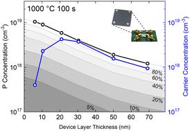
超薄绝缘体上硅(SOI)衬底的原位掺杂是通过使用含有掺杂分子的聚合物来实现的。在厚度值 (HSOI) 为 6 至 70 nm 的逐渐变薄的器件层中,研究了相同 P 剂量(1 × 1013 cm-2)下 P 杂质原子的注入情况。掺杂剂浓度是通过飞行时间二次离子质谱 (ToF-SIMS) 测量确定的。样品电阻率 (ρ)、载流子浓度 (ne) 和迁移率 (μ)是结合范-德-保尔配置中的片电阻和霍尔测量结果确定的。在 HSOI ≥ 30 nm 的样品中,注入的掺杂剂在室温下几乎完全活化和电离。当器件层厚度减小时,电离分数逐渐下降到 5%。掺杂剂的不完全电离伴随着电子迁移率的增加,其值远远大于已报道的块状硅的迁移率。在 HSOI > 20 nm 的 SOI 样品中,Altermatt 等人的三维体模型完美地描述了室温下电离 P 原子的比例。
Donor incomplete ionization and mobility enhancement in ultra-thin silicon-on-insulator films doped by phosphorus end-terminated polymers
Ex situ doping of ultra-thin silicon-on-insulator (SOI) substrates is performed by using polymers terminated with a doping containing moiety. The injection of P impurity atoms is investigated confining the same P dose of ∼ 1 × 1013 cm−2 in a progressively thinner device layer, with thickness values (HSOI) from 6 to 70 nm. The dopant concentration is determined by Time-of-flight secondary ion mass spectroscopy (ToF-SIMS) measurements. Sample resistivity (ρ), carrier concentration (ne) and mobility (μ) are determined combining sheet resistance and Hall measurements in van der Pauw configuration. Almost complete activation and full ionization of the injected dopants is observed at room temperature in the samples with HSOI ≥ 30 nm. The ionization fraction progressively drops to 5% when reducing the thickness of the device layer. Dopant incomplete ionization is accompanied by an increase in electron mobility, with values significantly larger than those reported for bulk Si. In the SOI samples with HSOI > 20 nm, the fraction of ionized P atoms at room temperature is perfectly described by the 3D bulk model of Altermatt et al. For HSOI ≤ 20 nm, the bulk model must be corrected to account for the effect of interface states and dielectric mismatch between Si and surrounding SiO2.
期刊介绍:
The Journal of Materials Chemistry is divided into three distinct sections, A, B, and C, each catering to specific applications of the materials under study:
Journal of Materials Chemistry A focuses primarily on materials intended for applications in energy and sustainability.
Journal of Materials Chemistry B specializes in materials designed for applications in biology and medicine.
Journal of Materials Chemistry C is dedicated to materials suitable for applications in optical, magnetic, and electronic devices.
Example topic areas within the scope of Journal of Materials Chemistry C are listed below. This list is neither exhaustive nor exclusive.
Bioelectronics
Conductors
Detectors
Dielectrics
Displays
Ferroelectrics
Lasers
LEDs
Lighting
Liquid crystals
Memory
Metamaterials
Multiferroics
Photonics
Photovoltaics
Semiconductors
Sensors
Single molecule conductors
Spintronics
Superconductors
Thermoelectrics
Topological insulators
Transistors

 求助内容:
求助内容: 应助结果提醒方式:


