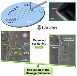
重复纳米划痕下单晶硅的变形特征和次表层损伤

IF 4.2 3区 工程技术 Q2 ENGINEERING, ELECTRICAL & ELECTRONIC
Yang He , Liangchi Zhang
{"title":"重复纳米划痕下单晶硅的变形特征和次表层损伤","authors":"Yang He ,&nbsp;Liangchi Zhang","doi":"10.1016/j.mssp.2024.109169","DOIUrl":null,"url":null,"abstract":"<div><div>In the context of grinding and polishing of monocrystalline silicon, abrasive particles repeatedly scratch the surface. The resultant subsurface damage significantly degrades the performance of monocrystalline silicon as a semiconductor substrate or optical component. However, the exact mechanism of material removal in monocrystalline silicon subjected to repeated nano-scratching remains inadequately understood. To address this gap, we conducted an in-depth study of the deformation characteristics of monocrystalline silicon via repeated nano-scratch tests. The nano-scratching was performed using atomic force microscopy (AFM) with a diamond tip, which had a radius of approximately 62 nm, under a normal load of about 23 μN. We employed scanning electron microscopy and transmission electron microscopy to analyze the states of the removed material, focusing on the mechanisms of material removal in ductile-regime machining. Our findings indicated that the monocrystalline silicon surface was removed through the formation of continuous curved chips composed of amorphous phase structures. Subsurface deformation from a single nano-scratching was through amorphization and machining defects, including dislocations, stacking faults, and lattice distortions. With repeated nano-scratching, these defects further underwent amorphization and became randomly distributed, rather than occurring in the &lt;111&gt; direction. Moreover, the subsurface defects exhibited a tendency not to expand or penetrate deeper with increasing nano-scratching cycles. This study provides crucial insights into the evolution of subsurface damage under repeated nano-scratching, offering valuable guidance for optimizing grinding and polishing processes to achieve high-quality subsurface and further enhance the performance of monocrystalline silicon.</div></div>","PeriodicalId":18240,"journal":{"name":"Materials Science in Semiconductor Processing","volume":"187 ","pages":"Article 109169"},"PeriodicalIF":4.2000,"publicationDate":"2024-11-26","publicationTypes":"Journal Article","fieldsOfStudy":null,"isOpenAccess":false,"openAccessPdf":"","citationCount":"0","resultStr":"{\"title\":\"Deformation characteristics and subsurface damage of monocrystalline silicon under repeated nano-scratching\",\"authors\":\"Yang He ,&nbsp;Liangchi Zhang\",\"doi\":\"10.1016/j.mssp.2024.109169\",\"DOIUrl\":null,\"url\":null,\"abstract\":\"<div><div>In the context of grinding and polishing of monocrystalline silicon, abrasive particles repeatedly scratch the surface. The resultant subsurface damage significantly degrades the performance of monocrystalline silicon as a semiconductor substrate or optical component. However, the exact mechanism of material removal in monocrystalline silicon subjected to repeated nano-scratching remains inadequately understood. To address this gap, we conducted an in-depth study of the deformation characteristics of monocrystalline silicon via repeated nano-scratch tests. The nano-scratching was performed using atomic force microscopy (AFM) with a diamond tip, which had a radius of approximately 62 nm, under a normal load of about 23 μN. We employed scanning electron microscopy and transmission electron microscopy to analyze the states of the removed material, focusing on the mechanisms of material removal in ductile-regime machining. Our findings indicated that the monocrystalline silicon surface was removed through the formation of continuous curved chips composed of amorphous phase structures. Subsurface deformation from a single nano-scratching was through amorphization and machining defects, including dislocations, stacking faults, and lattice distortions. With repeated nano-scratching, these defects further underwent amorphization and became randomly distributed, rather than occurring in the &lt;111&gt; direction. Moreover, the subsurface defects exhibited a tendency not to expand or penetrate deeper with increasing nano-scratching cycles. This study provides crucial insights into the evolution of subsurface damage under repeated nano-scratching, offering valuable guidance for optimizing grinding and polishing processes to achieve high-quality subsurface and further enhance the performance of monocrystalline silicon.</div></div>\",\"PeriodicalId\":18240,\"journal\":{\"name\":\"Materials Science in Semiconductor Processing\",\"volume\":\"187 \",\"pages\":\"Article 109169\"},\"PeriodicalIF\":4.2000,\"publicationDate\":\"2024-11-26\",\"publicationTypes\":\"Journal Article\",\"fieldsOfStudy\":null,\"isOpenAccess\":false,\"openAccessPdf\":\"\",\"citationCount\":\"0\",\"resultStr\":null,\"platform\":\"Semanticscholar\",\"paperid\":null,\"PeriodicalName\":\"Materials Science in Semiconductor Processing\",\"FirstCategoryId\":\"5\",\"ListUrlMain\":\"https://www.sciencedirect.com/science/article/pii/S1369800124010655\",\"RegionNum\":3,\"RegionCategory\":\"工程技术\",\"ArticlePicture\":[],\"TitleCN\":null,\"AbstractTextCN\":null,\"PMCID\":null,\"EPubDate\":\"\",\"PubModel\":\"\",\"JCR\":\"Q2\",\"JCRName\":\"ENGINEERING, ELECTRICAL & ELECTRONIC\",\"Score\":null,\"Total\":0}","platform":"Semanticscholar","paperid":null,"PeriodicalName":"Materials Science in Semiconductor Processing","FirstCategoryId":"5","ListUrlMain":"https://www.sciencedirect.com/science/article/pii/S1369800124010655","RegionNum":3,"RegionCategory":"工程技术","ArticlePicture":[],"TitleCN":null,"AbstractTextCN":null,"PMCID":null,"EPubDate":"","PubModel":"","JCR":"Q2","JCRName":"ENGINEERING, ELECTRICAL & ELECTRONIC","Score":null,"Total":0}
引用次数: 0

摘要

在对单晶硅进行研磨和抛光时,磨料颗粒会反复划伤其表面。由此造成的表面下损伤会大大降低单晶硅作为半导体衬底或光学元件的性能。然而,人们对单晶硅在反复纳米划痕作用下材料去除的确切机制仍缺乏足够的了解。针对这一空白,我们通过重复纳米划痕试验对单晶硅的变形特性进行了深入研究。我们使用原子力显微镜(AFM)和半径约为 62 nm 的金刚石针尖,在约 23 μN 的正常载荷下进行了纳米划痕试验。我们使用扫描电子显微镜和透射电子显微镜分析了被去除材料的状态,重点研究了韧性机理加工中的材料去除机制。我们的研究结果表明,单晶硅表面是通过形成由非晶相结构组成的连续弯曲切屑而被去除的。单次纳米划痕产生的次表面变形是通过非晶化和加工缺陷(包括位错、堆积断层和晶格畸变)产生的。随着纳米划痕的反复进行,这些缺陷进一步发生非晶化,并变得随机分布,而不是沿<111>方向出现。此外,随着纳米划痕周期的增加,表面下缺陷呈现出不扩展或不深入的趋势。这项研究对反复纳米划痕下的次表面损伤演变提供了重要的见解,为优化研磨和抛光工艺以获得高质量的次表面和进一步提高单晶硅的性能提供了宝贵的指导。
本文章由计算机程序翻译,如有差异,请以英文原文为准。

Deformation characteristics and subsurface damage of monocrystalline silicon under repeated nano-scratching

Deformation characteristics and subsurface damage of monocrystalline silicon under repeated nano-scratching
In the context of grinding and polishing of monocrystalline silicon, abrasive particles repeatedly scratch the surface. The resultant subsurface damage significantly degrades the performance of monocrystalline silicon as a semiconductor substrate or optical component. However, the exact mechanism of material removal in monocrystalline silicon subjected to repeated nano-scratching remains inadequately understood. To address this gap, we conducted an in-depth study of the deformation characteristics of monocrystalline silicon via repeated nano-scratch tests. The nano-scratching was performed using atomic force microscopy (AFM) with a diamond tip, which had a radius of approximately 62 nm, under a normal load of about 23 μN. We employed scanning electron microscopy and transmission electron microscopy to analyze the states of the removed material, focusing on the mechanisms of material removal in ductile-regime machining. Our findings indicated that the monocrystalline silicon surface was removed through the formation of continuous curved chips composed of amorphous phase structures. Subsurface deformation from a single nano-scratching was through amorphization and machining defects, including dislocations, stacking faults, and lattice distortions. With repeated nano-scratching, these defects further underwent amorphization and became randomly distributed, rather than occurring in the <111> direction. Moreover, the subsurface defects exhibited a tendency not to expand or penetrate deeper with increasing nano-scratching cycles. This study provides crucial insights into the evolution of subsurface damage under repeated nano-scratching, offering valuable guidance for optimizing grinding and polishing processes to achieve high-quality subsurface and further enhance the performance of monocrystalline silicon.
求助全文
通过发布文献求助,成功后即可免费获取论文全文。 去求助
来源期刊
Materials Science in Semiconductor Processing
Materials Science in Semiconductor Processing 工程技术-材料科学:综合
CiteScore
8.00
自引率
4.90%
发文量
780
审稿时长
42 days
期刊介绍: Materials Science in Semiconductor Processing provides a unique forum for the discussion of novel processing, applications and theoretical studies of functional materials and devices for (opto)electronics, sensors, detectors, biotechnology and green energy. Each issue will aim to provide a snapshot of current insights, new achievements, breakthroughs and future trends in such diverse fields as microelectronics, energy conversion and storage, communications, biotechnology, (photo)catalysis, nano- and thin-film technology, hybrid and composite materials, chemical processing, vapor-phase deposition, device fabrication, and modelling, which are the backbone of advanced semiconductor processing and applications. Coverage will include: advanced lithography for submicron devices; etching and related topics; ion implantation; damage evolution and related issues; plasma and thermal CVD; rapid thermal processing; advanced metallization and interconnect schemes; thin dielectric layers, oxidation; sol-gel processing; chemical bath and (electro)chemical deposition; compound semiconductor processing; new non-oxide materials and their applications; (macro)molecular and hybrid materials; molecular dynamics, ab-initio methods, Monte Carlo, etc.; new materials and processes for discrete and integrated circuits; magnetic materials and spintronics; heterostructures and quantum devices; engineering of the electrical and optical properties of semiconductors; crystal growth mechanisms; reliability, defect density, intrinsic impurities and defects.
×
引用
GB/T 7714-2015
复制
MLA
复制
APA
复制
导出至
BibTeX EndNote RefMan NoteFirst NoteExpress
×
提示
您的信息不完整,为了账户安全,请先补充。
现在去补充
×
提示
您因"违规操作"
具体请查看互助需知
我知道了
×
提示
确定
请完成安全验证×
copy
已复制链接
快去分享给好友吧!
我知道了
右上角分享
点击右上角分享
0
联系我们:info@booksci.cn Book学术提供免费学术资源搜索服务,方便国内外学者检索中英文文献。致力于提供最便捷和优质的服务体验。 Copyright © 2023 布克学术 All rights reserved.
京ICP备2023020795号-1
ghs 京公网安备 11010802042870号
Book学术文献互助
Book学术文献互助群
群 号:481959085
Book学术官方微信