Dani George , H.R. Chandan , R. Shwetharani , M. Faisal , Jahir Ahmed , Farid A. Harraz , R. Geetha Balakrishna
{"title":"了解石墨;理论见解及其光电行为","authors":"Dani George , H.R. Chandan , R. Shwetharani , M. Faisal , Jahir Ahmed , Farid A. Harraz , R. Geetha Balakrishna","doi":"10.1016/j.mssp.2024.109113","DOIUrl":null,"url":null,"abstract":"<div><div>Two-dimensional Graphynes (GYs) exhibit extraordinary properties, owing to the highly conjugated doubly and triply bonded carbon atoms in the hexagonal lattice. Recently, γ-GYs have attracted tremendous interest due to its exciting electrical and optical properties and it is necessary to comprehend these properties for future research in this field. This review focus on discussing the fundamental chemistry of the combination of <em>sp</em> and <em>sp</em><sup>2</sup> hybridization in GYs that contributes to its unique properties, particularly opto electrochemical properties of GYs. A detailed track record against a set of properties for developing efficient GYs based materials will help us look ahead in the right direction. The theoretical analysis of the electronic band structure of GYs, stability in relation to <em>sp</em> hybridization, experimental techniques used to tune their optical bandgap, and to improve mobility and carrier lifetimes, are covered in this review. The review then lists the merits of using GYs in various photo and electrochemical applications. Finally, current difficulties and future prospects for using these materials for the specified purpose are discussed.</div></div>","PeriodicalId":18240,"journal":{"name":"Materials Science in Semiconductor Processing","volume":"187 ","pages":"Article 109113"},"PeriodicalIF":4.2000,"publicationDate":"2024-11-24","publicationTypes":"Journal Article","fieldsOfStudy":null,"isOpenAccess":false,"openAccessPdf":"","citationCount":"0","resultStr":"{\"title\":\"Understanding graphyne; theoretical insights and its optoelectronic behaviour\",\"authors\":\"Dani George , H.R. Chandan , R. Shwetharani , M. Faisal , Jahir Ahmed , Farid A. Harraz , R. Geetha Balakrishna\",\"doi\":\"10.1016/j.mssp.2024.109113\",\"DOIUrl\":null,\"url\":null,\"abstract\":\"<div><div>Two-dimensional Graphynes (GYs) exhibit extraordinary properties, owing to the highly conjugated doubly and triply bonded carbon atoms in the hexagonal lattice. Recently, γ-GYs have attracted tremendous interest due to its exciting electrical and optical properties and it is necessary to comprehend these properties for future research in this field. This review focus on discussing the fundamental chemistry of the combination of <em>sp</em> and <em>sp</em><sup>2</sup> hybridization in GYs that contributes to its unique properties, particularly opto electrochemical properties of GYs. A detailed track record against a set of properties for developing efficient GYs based materials will help us look ahead in the right direction. The theoretical analysis of the electronic band structure of GYs, stability in relation to <em>sp</em> hybridization, experimental techniques used to tune their optical bandgap, and to improve mobility and carrier lifetimes, are covered in this review. The review then lists the merits of using GYs in various photo and electrochemical applications. Finally, current difficulties and future prospects for using these materials for the specified purpose are discussed.</div></div>\",\"PeriodicalId\":18240,\"journal\":{\"name\":\"Materials Science in Semiconductor Processing\",\"volume\":\"187 \",\"pages\":\"Article 109113\"},\"PeriodicalIF\":4.2000,\"publicationDate\":\"2024-11-24\",\"publicationTypes\":\"Journal Article\",\"fieldsOfStudy\":null,\"isOpenAccess\":false,\"openAccessPdf\":\"\",\"citationCount\":\"0\",\"resultStr\":null,\"platform\":\"Semanticscholar\",\"paperid\":null,\"PeriodicalName\":\"Materials Science in Semiconductor Processing\",\"FirstCategoryId\":\"5\",\"ListUrlMain\":\"https://www.sciencedirect.com/science/article/pii/S1369800124010096\",\"RegionNum\":3,\"RegionCategory\":\"工程技术\",\"ArticlePicture\":[],\"TitleCN\":null,\"AbstractTextCN\":null,\"PMCID\":null,\"EPubDate\":\"\",\"PubModel\":\"\",\"JCR\":\"Q2\",\"JCRName\":\"ENGINEERING, ELECTRICAL & ELECTRONIC\",\"Score\":null,\"Total\":0}","platform":"Semanticscholar","paperid":null,"PeriodicalName":"Materials Science in Semiconductor Processing","FirstCategoryId":"5","ListUrlMain":"https://www.sciencedirect.com/science/article/pii/S1369800124010096","RegionNum":3,"RegionCategory":"工程技术","ArticlePicture":[],"TitleCN":null,"AbstractTextCN":null,"PMCID":null,"EPubDate":"","PubModel":"","JCR":"Q2","JCRName":"ENGINEERING, ELECTRICAL & ELECTRONIC","Score":null,"Total":0}
Understanding graphyne; theoretical insights and its optoelectronic behaviour
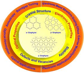
Two-dimensional Graphynes (GYs) exhibit extraordinary properties, owing to the highly conjugated doubly and triply bonded carbon atoms in the hexagonal lattice. Recently, γ-GYs have attracted tremendous interest due to its exciting electrical and optical properties and it is necessary to comprehend these properties for future research in this field. This review focus on discussing the fundamental chemistry of the combination of sp and sp2 hybridization in GYs that contributes to its unique properties, particularly opto electrochemical properties of GYs. A detailed track record against a set of properties for developing efficient GYs based materials will help us look ahead in the right direction. The theoretical analysis of the electronic band structure of GYs, stability in relation to sp hybridization, experimental techniques used to tune their optical bandgap, and to improve mobility and carrier lifetimes, are covered in this review. The review then lists the merits of using GYs in various photo and electrochemical applications. Finally, current difficulties and future prospects for using these materials for the specified purpose are discussed.
期刊介绍:
Materials Science in Semiconductor Processing provides a unique forum for the discussion of novel processing, applications and theoretical studies of functional materials and devices for (opto)electronics, sensors, detectors, biotechnology and green energy.
Each issue will aim to provide a snapshot of current insights, new achievements, breakthroughs and future trends in such diverse fields as microelectronics, energy conversion and storage, communications, biotechnology, (photo)catalysis, nano- and thin-film technology, hybrid and composite materials, chemical processing, vapor-phase deposition, device fabrication, and modelling, which are the backbone of advanced semiconductor processing and applications.
Coverage will include: advanced lithography for submicron devices; etching and related topics; ion implantation; damage evolution and related issues; plasma and thermal CVD; rapid thermal processing; advanced metallization and interconnect schemes; thin dielectric layers, oxidation; sol-gel processing; chemical bath and (electro)chemical deposition; compound semiconductor processing; new non-oxide materials and their applications; (macro)molecular and hybrid materials; molecular dynamics, ab-initio methods, Monte Carlo, etc.; new materials and processes for discrete and integrated circuits; magnetic materials and spintronics; heterostructures and quantum devices; engineering of the electrical and optical properties of semiconductors; crystal growth mechanisms; reliability, defect density, intrinsic impurities and defects.