加速建立硅酞菁 OFET 薄膜加工与性能关系的快速原型技术

IF 5.3 2区 材料科学 Q2 MATERIALS SCIENCE, MULTIDISCIPLINARY
Rosemary R. Cranston, Jacob Mauthe, Tonghui Wang, Gaurab J. Thapa, Aram Amassian, Benoît H. Lessard
{"title":"加速建立硅酞菁 OFET 薄膜加工与性能关系的快速原型技术","authors":"Rosemary R. Cranston, Jacob Mauthe, Tonghui Wang, Gaurab J. Thapa, Aram Amassian, Benoît H. Lessard","doi":"10.1002/aelm.202400500","DOIUrl":null,"url":null,"abstract":"Understanding the complex relationships underlying the performance of organic electronic devices, such as organic field‐effect transistors (OFETs), requires researchers to navigate a multi‐dimensional parameter space that includes material design, solution formulation, fabrication parameters, and device geometry. Herein, a recently developed materials acceleration platform is demonstrated, named the RoboMapper, to perform direct on‐chip fabrication of OFETs by ultrasonic meniscus printing using silicon phthalocyanine (SiPc) derivatives as the semiconductor. OFETs using bis(tri‐<jats:italic>n</jats:italic>‐butylsilyl oxide) SiPc ((3BS)<jats:sub>2</jats:sub>‐SiPc) exhibited the best device performance characterized by the highest electron field‐effect mobility (<jats:italic>µ<jats:sub>e</jats:sub></jats:italic>). Through optical microscopy and grazing‐incidence wide‐angle X‐ray scattering (GIWAXS), the favorable performance of (3BS)<jats:sub>2</jats:sub>‐SiPc is attributed to the specific film morphology and molecular packing achieved with optimal print conditions. Investigating the impact of deposition parameters reveals the crucial role of solvent evaporation rate and print speed in achieving high‐quality film formation. Overall, optimal fabrication conditions for (3BS)<jats:sub>2</jats:sub>‐SiPc devices include slow print speeds and fast evaporating solutions achieved by using a mixture of co‐solvents and an elevated substrate temperature. The results of this work reveal distinct relationships between deposition conditions, film properties, and device performance for each SiPc derivative and emphasize the necessity of high throughput experimentation to comprehensively understand process‐performance relationships in organic semiconductors.","PeriodicalId":110,"journal":{"name":"Advanced Electronic Materials","volume":"8 1","pages":""},"PeriodicalIF":5.3000,"publicationDate":"2024-11-18","publicationTypes":"Journal Article","fieldsOfStudy":null,"isOpenAccess":false,"openAccessPdf":"","citationCount":"0","resultStr":"{\"title\":\"Rapid Prototyping for Accelerated Establishment of Film Processing‐Performance Relationships in Silicon Phthalocyanine OFETs\",\"authors\":\"Rosemary R. Cranston, Jacob Mauthe, Tonghui Wang, Gaurab J. Thapa, Aram Amassian, Benoît H. Lessard\",\"doi\":\"10.1002/aelm.202400500\",\"DOIUrl\":null,\"url\":null,\"abstract\":\"Understanding the complex relationships underlying the performance of organic electronic devices, such as organic field‐effect transistors (OFETs), requires researchers to navigate a multi‐dimensional parameter space that includes material design, solution formulation, fabrication parameters, and device geometry. Herein, a recently developed materials acceleration platform is demonstrated, named the RoboMapper, to perform direct on‐chip fabrication of OFETs by ultrasonic meniscus printing using silicon phthalocyanine (SiPc) derivatives as the semiconductor. OFETs using bis(tri‐<jats:italic>n</jats:italic>‐butylsilyl oxide) SiPc ((3BS)<jats:sub>2</jats:sub>‐SiPc) exhibited the best device performance characterized by the highest electron field‐effect mobility (<jats:italic>µ<jats:sub>e</jats:sub></jats:italic>). Through optical microscopy and grazing‐incidence wide‐angle X‐ray scattering (GIWAXS), the favorable performance of (3BS)<jats:sub>2</jats:sub>‐SiPc is attributed to the specific film morphology and molecular packing achieved with optimal print conditions. Investigating the impact of deposition parameters reveals the crucial role of solvent evaporation rate and print speed in achieving high‐quality film formation. Overall, optimal fabrication conditions for (3BS)<jats:sub>2</jats:sub>‐SiPc devices include slow print speeds and fast evaporating solutions achieved by using a mixture of co‐solvents and an elevated substrate temperature. The results of this work reveal distinct relationships between deposition conditions, film properties, and device performance for each SiPc derivative and emphasize the necessity of high throughput experimentation to comprehensively understand process‐performance relationships in organic semiconductors.\",\"PeriodicalId\":110,\"journal\":{\"name\":\"Advanced Electronic Materials\",\"volume\":\"8 1\",\"pages\":\"\"},\"PeriodicalIF\":5.3000,\"publicationDate\":\"2024-11-18\",\"publicationTypes\":\"Journal Article\",\"fieldsOfStudy\":null,\"isOpenAccess\":false,\"openAccessPdf\":\"\",\"citationCount\":\"0\",\"resultStr\":null,\"platform\":\"Semanticscholar\",\"paperid\":null,\"PeriodicalName\":\"Advanced Electronic Materials\",\"FirstCategoryId\":\"88\",\"ListUrlMain\":\"https://doi.org/10.1002/aelm.202400500\",\"RegionNum\":2,\"RegionCategory\":\"材料科学\",\"ArticlePicture\":[],\"TitleCN\":null,\"AbstractTextCN\":null,\"PMCID\":null,\"EPubDate\":\"\",\"PubModel\":\"\",\"JCR\":\"Q2\",\"JCRName\":\"MATERIALS SCIENCE, MULTIDISCIPLINARY\",\"Score\":null,\"Total\":0}","platform":"Semanticscholar","paperid":null,"PeriodicalName":"Advanced Electronic Materials","FirstCategoryId":"88","ListUrlMain":"https://doi.org/10.1002/aelm.202400500","RegionNum":2,"RegionCategory":"材料科学","ArticlePicture":[],"TitleCN":null,"AbstractTextCN":null,"PMCID":null,"EPubDate":"","PubModel":"","JCR":"Q2","JCRName":"MATERIALS SCIENCE, MULTIDISCIPLINARY","Score":null,"Total":0}
引用次数: 0

摘要

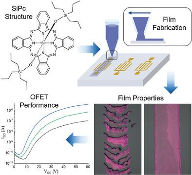
要了解有机场效应晶体管(OFET)等有机电子器件性能背后的复杂关系,研究人员需要浏览多维参数空间,其中包括材料设计、溶液配方、制造参数和器件几何形状。本文展示了最近开发的一种名为 RoboMapper 的材料加速平台,该平台可使用硅酞菁(SiPc)衍生物作为半导体,通过超声波半月板印刷直接在芯片上制造 OFET。使用双(三正丁基氧化硅)SiPc((3BS)2-SiPc)的 OFET 表现出最佳的器件性能,其特点是电子场效应迁移率(µe)最高。通过光学显微镜和掠入射广角 X 射线散射 (GIWAXS),(3BS)2-SiPc 的良好性能归功于在最佳印刷条件下实现的特定薄膜形貌和分子堆积。对沉积参数影响的研究表明,溶剂蒸发率和印刷速度对实现高质量薄膜形成起着至关重要的作用。总体而言,(3BS)2-SiPc 器件的最佳制造条件包括较慢的打印速度和快速蒸发溶液,通过使用混合助溶剂和升高基底温度来实现。这项工作的结果揭示了每种 SiPc 衍生物的沉积条件、薄膜特性和器件性能之间的独特关系,并强调了高通量实验对全面了解有机半导体工艺性能关系的必要性。
本文章由计算机程序翻译,如有差异,请以英文原文为准。

Rapid Prototyping for Accelerated Establishment of Film Processing‐Performance Relationships in Silicon Phthalocyanine OFETs

Rapid Prototyping for Accelerated Establishment of Film Processing‐Performance Relationships in Silicon Phthalocyanine OFETs
Understanding the complex relationships underlying the performance of organic electronic devices, such as organic field‐effect transistors (OFETs), requires researchers to navigate a multi‐dimensional parameter space that includes material design, solution formulation, fabrication parameters, and device geometry. Herein, a recently developed materials acceleration platform is demonstrated, named the RoboMapper, to perform direct on‐chip fabrication of OFETs by ultrasonic meniscus printing using silicon phthalocyanine (SiPc) derivatives as the semiconductor. OFETs using bis(tri‐n‐butylsilyl oxide) SiPc ((3BS)2‐SiPc) exhibited the best device performance characterized by the highest electron field‐effect mobility (µe). Through optical microscopy and grazing‐incidence wide‐angle X‐ray scattering (GIWAXS), the favorable performance of (3BS)2‐SiPc is attributed to the specific film morphology and molecular packing achieved with optimal print conditions. Investigating the impact of deposition parameters reveals the crucial role of solvent evaporation rate and print speed in achieving high‐quality film formation. Overall, optimal fabrication conditions for (3BS)2‐SiPc devices include slow print speeds and fast evaporating solutions achieved by using a mixture of co‐solvents and an elevated substrate temperature. The results of this work reveal distinct relationships between deposition conditions, film properties, and device performance for each SiPc derivative and emphasize the necessity of high throughput experimentation to comprehensively understand process‐performance relationships in organic semiconductors.
求助全文
通过发布文献求助,成功后即可免费获取论文全文。 去求助
来源期刊
Advanced Electronic Materials
Advanced Electronic Materials NANOSCIENCE & NANOTECHNOLOGYMATERIALS SCIE-MATERIALS SCIENCE, MULTIDISCIPLINARY
CiteScore
11.00
自引率
3.20%
发文量
433
期刊介绍: Advanced Electronic Materials is an interdisciplinary forum for peer-reviewed, high-quality, high-impact research in the fields of materials science, physics, and engineering of electronic and magnetic materials. It includes research on physics and physical properties of electronic and magnetic materials, spintronics, electronics, device physics and engineering, micro- and nano-electromechanical systems, and organic electronics, in addition to fundamental research.
×
引用
GB/T 7714-2015
复制
MLA
复制
APA
复制
导出至
BibTeX EndNote RefMan NoteFirst NoteExpress
×
提示
您的信息不完整,为了账户安全,请先补充。
现在去补充
×
提示
您因"违规操作"
具体请查看互助需知
我知道了
×
提示
确定
请完成安全验证×
copy
已复制链接
快去分享给好友吧!
我知道了
右上角分享
点击右上角分享
0
联系我们:info@booksci.cn Book学术提供免费学术资源搜索服务,方便国内外学者检索中英文文献。致力于提供最便捷和优质的服务体验。 Copyright © 2023 布克学术 All rights reserved.
京ICP备2023020795号-1
ghs 京公网安备 11010802042870号
Book学术文献互助
Book学术文献互助群
群 号:481959085
Book学术官方微信