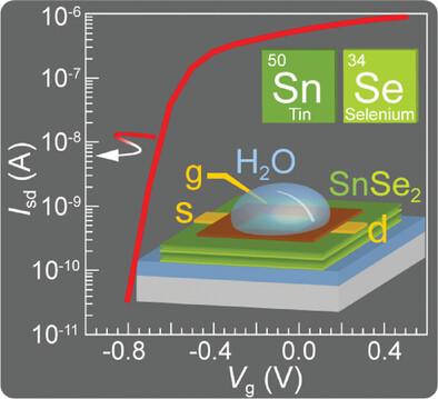
具有超低次阈值波动和栅极控制光电导切换功能的高迁移率、高载流子密度 SnSe2 场效应晶体管

IF 5.3 2区 材料科学 Q2 MATERIALS SCIENCE, MULTIDISCIPLINARY
Yuan Huang, Eli Sutter, Bruce A. Parkinson, Peter Sutter
{"title":"具有超低次阈值波动和栅极控制光电导切换功能的高迁移率、高载流子密度 SnSe2 场效应晶体管","authors":"Yuan Huang, Eli Sutter, Bruce A. Parkinson, Peter Sutter","doi":"10.1002/aelm.202400691","DOIUrl":null,"url":null,"abstract":"2D and layered semiconductors are considered as promising electronic materials, particularly for applications that require high carrier mobility and efficient field‐effect switching combined with mechanical flexibility. To date, however, the highest mobility has been realized primarily at low carrier concentration. Here, it is shown that few‐layer/multilayer SnSe<jats:sub>2</jats:sub> gated by a solution top gate combines very high room‐temperature electron mobility (up to 800 cm<jats:sup>2</jats:sup> V<jats:sup>−1</jats:sup>s<jats:sup>−1</jats:sup>), along with large on‐off current ratios (&gt;10<jats:sup>5</jats:sup>) and a subthreshold swing below the thermodynamic limit (50 mV per decade) in field‐effect devices, at exceptionally large sheet carrier concentrations of ≈10<jats:sup>13</jats:sup> cm<jats:sup>−2</jats:sup>. Observed mobility enhancements upon partial depletion of the channel point to near‐surface defects or impurities as the mobility‐limiting scattering centers. Under illumination, the resulting gap states give rise to gate‐controlled switching between positive and negative photoconductance. The results qualify SnSe<jats:sub>2</jats:sub> as a promising layered semiconductor for flexible and wearable electronics, as well as for the realization of advanced approaches to photodetection.","PeriodicalId":110,"journal":{"name":"Advanced Electronic Materials","volume":"64 1","pages":""},"PeriodicalIF":5.3000,"publicationDate":"2024-11-18","publicationTypes":"Journal Article","fieldsOfStudy":null,"isOpenAccess":false,"openAccessPdf":"","citationCount":"0","resultStr":"{\"title\":\"High Mobility, High Carrier Density SnSe2 Field‐Effect Transistors with Ultralow Subthreshold Swing and Gate‐Controlled Photoconductance Switching\",\"authors\":\"Yuan Huang, Eli Sutter, Bruce A. Parkinson, Peter Sutter\",\"doi\":\"10.1002/aelm.202400691\",\"DOIUrl\":null,\"url\":null,\"abstract\":\"2D and layered semiconductors are considered as promising electronic materials, particularly for applications that require high carrier mobility and efficient field‐effect switching combined with mechanical flexibility. To date, however, the highest mobility has been realized primarily at low carrier concentration. Here, it is shown that few‐layer/multilayer SnSe<jats:sub>2</jats:sub> gated by a solution top gate combines very high room‐temperature electron mobility (up to 800 cm<jats:sup>2</jats:sup> V<jats:sup>−1</jats:sup>s<jats:sup>−1</jats:sup>), along with large on‐off current ratios (&gt;10<jats:sup>5</jats:sup>) and a subthreshold swing below the thermodynamic limit (50 mV per decade) in field‐effect devices, at exceptionally large sheet carrier concentrations of ≈10<jats:sup>13</jats:sup> cm<jats:sup>−2</jats:sup>. Observed mobility enhancements upon partial depletion of the channel point to near‐surface defects or impurities as the mobility‐limiting scattering centers. Under illumination, the resulting gap states give rise to gate‐controlled switching between positive and negative photoconductance. The results qualify SnSe<jats:sub>2</jats:sub> as a promising layered semiconductor for flexible and wearable electronics, as well as for the realization of advanced approaches to photodetection.\",\"PeriodicalId\":110,\"journal\":{\"name\":\"Advanced Electronic Materials\",\"volume\":\"64 1\",\"pages\":\"\"},\"PeriodicalIF\":5.3000,\"publicationDate\":\"2024-11-18\",\"publicationTypes\":\"Journal Article\",\"fieldsOfStudy\":null,\"isOpenAccess\":false,\"openAccessPdf\":\"\",\"citationCount\":\"0\",\"resultStr\":null,\"platform\":\"Semanticscholar\",\"paperid\":null,\"PeriodicalName\":\"Advanced Electronic Materials\",\"FirstCategoryId\":\"88\",\"ListUrlMain\":\"https://doi.org/10.1002/aelm.202400691\",\"RegionNum\":2,\"RegionCategory\":\"材料科学\",\"ArticlePicture\":[],\"TitleCN\":null,\"AbstractTextCN\":null,\"PMCID\":null,\"EPubDate\":\"\",\"PubModel\":\"\",\"JCR\":\"Q2\",\"JCRName\":\"MATERIALS SCIENCE, MULTIDISCIPLINARY\",\"Score\":null,\"Total\":0}","platform":"Semanticscholar","paperid":null,"PeriodicalName":"Advanced Electronic Materials","FirstCategoryId":"88","ListUrlMain":"https://doi.org/10.1002/aelm.202400691","RegionNum":2,"RegionCategory":"材料科学","ArticlePicture":[],"TitleCN":null,"AbstractTextCN":null,"PMCID":null,"EPubDate":"","PubModel":"","JCR":"Q2","JCRName":"MATERIALS SCIENCE, MULTIDISCIPLINARY","Score":null,"Total":0}
引用次数: 0

摘要

二维和层状半导体被认为是前景广阔的电子材料,特别是在需要高载流子迁移率、高效场效应开关和机械灵活性的应用领域。然而,迄今为止,最高的迁移率主要是在低载流子浓度下实现的。这里的研究表明,采用溶液顶栅栅封的少层/多层 SnSe2 在室温下具有极高的电子迁移率(高达 800 cm2 V-1s-1),同时还具有较大的导通电流比(>105)和低于场效应器件热力学极限的亚阈值摆动(每10年 50 mV),而且片状载流子浓度特别大(≈1013 cm-2)。在沟道部分耗尽时观察到的迁移率增强表明,近表面缺陷或杂质是限制迁移率的散射中心。在光照下,由此产生的间隙态会导致正负光电导之间的栅极控制切换。研究结果证明,SnSe2 是一种很有前途的层状半导体,可用于柔性和可穿戴电子设备,以及实现先进的光检测方法。
本文章由计算机程序翻译,如有差异,请以英文原文为准。

High Mobility, High Carrier Density SnSe2 Field‐Effect Transistors with Ultralow Subthreshold Swing and Gate‐Controlled Photoconductance Switching

High Mobility, High Carrier Density SnSe2 Field‐Effect Transistors with Ultralow Subthreshold Swing and Gate‐Controlled Photoconductance Switching
2D and layered semiconductors are considered as promising electronic materials, particularly for applications that require high carrier mobility and efficient field‐effect switching combined with mechanical flexibility. To date, however, the highest mobility has been realized primarily at low carrier concentration. Here, it is shown that few‐layer/multilayer SnSe2 gated by a solution top gate combines very high room‐temperature electron mobility (up to 800 cm2 V−1s−1), along with large on‐off current ratios (>105) and a subthreshold swing below the thermodynamic limit (50 mV per decade) in field‐effect devices, at exceptionally large sheet carrier concentrations of ≈1013 cm−2. Observed mobility enhancements upon partial depletion of the channel point to near‐surface defects or impurities as the mobility‐limiting scattering centers. Under illumination, the resulting gap states give rise to gate‐controlled switching between positive and negative photoconductance. The results qualify SnSe2 as a promising layered semiconductor for flexible and wearable electronics, as well as for the realization of advanced approaches to photodetection.
求助全文
通过发布文献求助,成功后即可免费获取论文全文。 去求助
来源期刊
Advanced Electronic Materials
Advanced Electronic Materials NANOSCIENCE & NANOTECHNOLOGYMATERIALS SCIE-MATERIALS SCIENCE, MULTIDISCIPLINARY
CiteScore
11.00
自引率
3.20%
发文量
433
期刊介绍: Advanced Electronic Materials is an interdisciplinary forum for peer-reviewed, high-quality, high-impact research in the fields of materials science, physics, and engineering of electronic and magnetic materials. It includes research on physics and physical properties of electronic and magnetic materials, spintronics, electronics, device physics and engineering, micro- and nano-electromechanical systems, and organic electronics, in addition to fundamental research.
×
引用
GB/T 7714-2015
复制
MLA
复制
APA
复制
导出至
BibTeX EndNote RefMan NoteFirst NoteExpress
×
提示
您的信息不完整,为了账户安全,请先补充。
现在去补充
×
提示
您因"违规操作"
具体请查看互助需知
我知道了
×
提示
确定
请完成安全验证×
copy
已复制链接
快去分享给好友吧!
我知道了
右上角分享
点击右上角分享
0
联系我们:info@booksci.cn Book学术提供免费学术资源搜索服务,方便国内外学者检索中英文文献。致力于提供最便捷和优质的服务体验。 Copyright © 2023 布克学术 All rights reserved.
京ICP备2023020795号-1
ghs 京公网安备 11010802042870号
Book学术文献互助
Book学术文献互助群
群 号:481959085
Book学术官方微信