Xingkun Wang, Taoli Guo, Yiyang Shan, Ou Zhang, Hong Dong, Jincheng Liu and Feng Luo
{"title":"用于分子层沉积先进光刻技术的铝基混合薄膜光刻胶†。","authors":"Xingkun Wang, Taoli Guo, Yiyang Shan, Ou Zhang, Hong Dong, Jincheng Liu and Feng Luo","doi":"10.1039/D4TC02794A","DOIUrl":null,"url":null,"abstract":"<p >In the realm of advanced integrated circuits, the demand for novel resist materials becomes paramount as we progress toward smaller process nodes. Inorganic photoresists have received widespread attention due to their higher absorption of extreme ultraviolet (EUV) light and higher etch resistance. In our study, we employed trimethylaluminum (TMA) and 2-butene-1,4-diol (BED) <em>via</em> molecular layer deposition (MLD) to deposit an Al-based hybrid film coined “TMA–BED,” serving as an electron-beam photoresist. Through inductively coupled plasma (ICP) etching for resistance testing, the TMA–BED film exhibited exceptional selectivity with Si etching, reaching a minimum of ∼86, surpassing traditional photoresists by 14 times. Sensitivity and resolution were assessed using electron-beam lithography with 10 wt% ammonia as the developer, revealing a sensitivity of 450 μC cm<small><sup>−2</sup></small> at 2 keV and the capacity to resolve 10 nm line widths at 50 keV. Our results underscore the tremendous potential of TMA–BED hybrid films, deposited through MLD, for advanced lithographic techniques.</p>","PeriodicalId":84,"journal":{"name":"Journal of Materials Chemistry C","volume":" 43","pages":" 17544-17553"},"PeriodicalIF":5.7000,"publicationDate":"2024-09-18","publicationTypes":"Journal Article","fieldsOfStudy":null,"isOpenAccess":false,"openAccessPdf":"","citationCount":"0","resultStr":"{\"title\":\"An aluminum-based hybrid film photoresist for advanced lithography by molecular layer deposition†\",\"authors\":\"Xingkun Wang, Taoli Guo, Yiyang Shan, Ou Zhang, Hong Dong, Jincheng Liu and Feng Luo\",\"doi\":\"10.1039/D4TC02794A\",\"DOIUrl\":null,\"url\":null,\"abstract\":\"<p >In the realm of advanced integrated circuits, the demand for novel resist materials becomes paramount as we progress toward smaller process nodes. Inorganic photoresists have received widespread attention due to their higher absorption of extreme ultraviolet (EUV) light and higher etch resistance. In our study, we employed trimethylaluminum (TMA) and 2-butene-1,4-diol (BED) <em>via</em> molecular layer deposition (MLD) to deposit an Al-based hybrid film coined “TMA–BED,” serving as an electron-beam photoresist. Through inductively coupled plasma (ICP) etching for resistance testing, the TMA–BED film exhibited exceptional selectivity with Si etching, reaching a minimum of ∼86, surpassing traditional photoresists by 14 times. Sensitivity and resolution were assessed using electron-beam lithography with 10 wt% ammonia as the developer, revealing a sensitivity of 450 μC cm<small><sup>−2</sup></small> at 2 keV and the capacity to resolve 10 nm line widths at 50 keV. Our results underscore the tremendous potential of TMA–BED hybrid films, deposited through MLD, for advanced lithographic techniques.</p>\",\"PeriodicalId\":84,\"journal\":{\"name\":\"Journal of Materials Chemistry C\",\"volume\":\" 43\",\"pages\":\" 17544-17553\"},\"PeriodicalIF\":5.7000,\"publicationDate\":\"2024-09-18\",\"publicationTypes\":\"Journal Article\",\"fieldsOfStudy\":null,\"isOpenAccess\":false,\"openAccessPdf\":\"\",\"citationCount\":\"0\",\"resultStr\":null,\"platform\":\"Semanticscholar\",\"paperid\":null,\"PeriodicalName\":\"Journal of Materials Chemistry C\",\"FirstCategoryId\":\"1\",\"ListUrlMain\":\"https://pubs.rsc.org/en/content/articlelanding/2024/tc/d4tc02794a\",\"RegionNum\":2,\"RegionCategory\":\"材料科学\",\"ArticlePicture\":[],\"TitleCN\":null,\"AbstractTextCN\":null,\"PMCID\":null,\"EPubDate\":\"\",\"PubModel\":\"\",\"JCR\":\"Q2\",\"JCRName\":\"MATERIALS SCIENCE, MULTIDISCIPLINARY\",\"Score\":null,\"Total\":0}","platform":"Semanticscholar","paperid":null,"PeriodicalName":"Journal of Materials Chemistry C","FirstCategoryId":"1","ListUrlMain":"https://pubs.rsc.org/en/content/articlelanding/2024/tc/d4tc02794a","RegionNum":2,"RegionCategory":"材料科学","ArticlePicture":[],"TitleCN":null,"AbstractTextCN":null,"PMCID":null,"EPubDate":"","PubModel":"","JCR":"Q2","JCRName":"MATERIALS SCIENCE, MULTIDISCIPLINARY","Score":null,"Total":0}
An aluminum-based hybrid film photoresist for advanced lithography by molecular layer deposition†
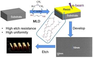
In the realm of advanced integrated circuits, the demand for novel resist materials becomes paramount as we progress toward smaller process nodes. Inorganic photoresists have received widespread attention due to their higher absorption of extreme ultraviolet (EUV) light and higher etch resistance. In our study, we employed trimethylaluminum (TMA) and 2-butene-1,4-diol (BED) via molecular layer deposition (MLD) to deposit an Al-based hybrid film coined “TMA–BED,” serving as an electron-beam photoresist. Through inductively coupled plasma (ICP) etching for resistance testing, the TMA–BED film exhibited exceptional selectivity with Si etching, reaching a minimum of ∼86, surpassing traditional photoresists by 14 times. Sensitivity and resolution were assessed using electron-beam lithography with 10 wt% ammonia as the developer, revealing a sensitivity of 450 μC cm−2 at 2 keV and the capacity to resolve 10 nm line widths at 50 keV. Our results underscore the tremendous potential of TMA–BED hybrid films, deposited through MLD, for advanced lithographic techniques.
期刊介绍:
The Journal of Materials Chemistry is divided into three distinct sections, A, B, and C, each catering to specific applications of the materials under study:
Journal of Materials Chemistry A focuses primarily on materials intended for applications in energy and sustainability.
Journal of Materials Chemistry B specializes in materials designed for applications in biology and medicine.
Journal of Materials Chemistry C is dedicated to materials suitable for applications in optical, magnetic, and electronic devices.
Example topic areas within the scope of Journal of Materials Chemistry C are listed below. This list is neither exhaustive nor exclusive.
Bioelectronics
Conductors
Detectors
Dielectrics
Displays
Ferroelectrics
Lasers
LEDs
Lighting
Liquid crystals
Memory
Metamaterials
Multiferroics
Photonics
Photovoltaics
Semiconductors
Sensors
Single molecule conductors
Spintronics
Superconductors
Thermoelectrics
Topological insulators
Transistors

 求助内容:
求助内容: 应助结果提醒方式:


