基于相变材料 VO2 和超材料石墨烯的太赫兹智能设备,兼具热调节吸收和选择性传输功能

IF 4.6 2区 物理与天体物理 Q1 OPTICS
Wenqiang Lu , Weiming Zhang , Qianju Song , Zao Yi , Shubo Cheng , Bin Tang , Qingdong Zeng , Pinghui Wu , Sohail Ahmad
{"title":"基于相变材料 VO2 和超材料石墨烯的太赫兹智能设备,兼具热调节吸收和选择性传输功能","authors":"Wenqiang Lu ,&nbsp;Weiming Zhang ,&nbsp;Qianju Song ,&nbsp;Zao Yi ,&nbsp;Shubo Cheng ,&nbsp;Bin Tang ,&nbsp;Qingdong Zeng ,&nbsp;Pinghui Wu ,&nbsp;Sohail Ahmad","doi":"10.1016/j.optlastec.2024.111928","DOIUrl":null,"url":null,"abstract":"<div><div>In this paper, a classical three-layer structure of proportionate terahertz intelligent device composed of vanadium dioxide and graphene is simulated and designed. The proportionate setting of this intelligent device allows for better control over the size of surface microstructures, thereby enhancing the utilization of materials during the production process. At a temperature of T = 345 K, the device exhibits perfect absorption efficiency of greater than or equal to 90 % in the frequency range of 2.46 THz to 6.85 THz (4.39 THz), spanning almost half of the terahertz band. At a temperature of T = 323 K, the device achieves absorption of over 77.3 % in the frequency range of 3.04 THz to 5.64 THz, with average transmittance rates of 69.61 % and 69.79 % in the frequency ranges of 0.01 THz to 2.32 THz and 6.82 THz to 10.00 THz, respectively. We use vanadium dioxide as the bottom layer to avoid the effect of traditional metal substrates that prevent electromagnetic waves from transmitting and limit the conversion of terahertz device performance. Temperature modulation enables control over absorption and transmission. We first explain the results based on the crystal structure within VO<sub>2</sub> and then analyze the surface electric field of the device at two temperatures using surface plasmons (SPs). By adjusting the structural parameters of the absorber and applying an external bias voltage, the Fermi energy of graphene can be altered, demonstrating the device’s physical coherence, manufacturing tolerance, and dynamic tuning capability. We investigate the influence of different incident angles of external electromagnetic waves on the device performance, showing that it maintains excellent performance over a wide range of angles, which is crucial for practical applications. Finally, we examined the implications of employing the Drude model to characterize silicon dioxide in the terahertz range and its potential impact on device performance. This holds significant implications for communication, detection, sensing, imaging, and provides insights for future terahertz device development.</div></div>","PeriodicalId":19511,"journal":{"name":"Optics and Laser Technology","volume":"181 ","pages":"Article 111928"},"PeriodicalIF":4.6000,"publicationDate":"2024-10-10","publicationTypes":"Journal Article","fieldsOfStudy":null,"isOpenAccess":false,"openAccessPdf":"","citationCount":"0","resultStr":"{\"title\":\"Terahertz smart devices based on phase change material VO2 and metamaterial graphene that combine thermally adjustable absorption and selective transmission\",\"authors\":\"Wenqiang Lu ,&nbsp;Weiming Zhang ,&nbsp;Qianju Song ,&nbsp;Zao Yi ,&nbsp;Shubo Cheng ,&nbsp;Bin Tang ,&nbsp;Qingdong Zeng ,&nbsp;Pinghui Wu ,&nbsp;Sohail Ahmad\",\"doi\":\"10.1016/j.optlastec.2024.111928\",\"DOIUrl\":null,\"url\":null,\"abstract\":\"<div><div>In this paper, a classical three-layer structure of proportionate terahertz intelligent device composed of vanadium dioxide and graphene is simulated and designed. The proportionate setting of this intelligent device allows for better control over the size of surface microstructures, thereby enhancing the utilization of materials during the production process. At a temperature of T = 345 K, the device exhibits perfect absorption efficiency of greater than or equal to 90 % in the frequency range of 2.46 THz to 6.85 THz (4.39 THz), spanning almost half of the terahertz band. At a temperature of T = 323 K, the device achieves absorption of over 77.3 % in the frequency range of 3.04 THz to 5.64 THz, with average transmittance rates of 69.61 % and 69.79 % in the frequency ranges of 0.01 THz to 2.32 THz and 6.82 THz to 10.00 THz, respectively. We use vanadium dioxide as the bottom layer to avoid the effect of traditional metal substrates that prevent electromagnetic waves from transmitting and limit the conversion of terahertz device performance. Temperature modulation enables control over absorption and transmission. We first explain the results based on the crystal structure within VO<sub>2</sub> and then analyze the surface electric field of the device at two temperatures using surface plasmons (SPs). By adjusting the structural parameters of the absorber and applying an external bias voltage, the Fermi energy of graphene can be altered, demonstrating the device’s physical coherence, manufacturing tolerance, and dynamic tuning capability. We investigate the influence of different incident angles of external electromagnetic waves on the device performance, showing that it maintains excellent performance over a wide range of angles, which is crucial for practical applications. Finally, we examined the implications of employing the Drude model to characterize silicon dioxide in the terahertz range and its potential impact on device performance. This holds significant implications for communication, detection, sensing, imaging, and provides insights for future terahertz device development.</div></div>\",\"PeriodicalId\":19511,\"journal\":{\"name\":\"Optics and Laser Technology\",\"volume\":\"181 \",\"pages\":\"Article 111928\"},\"PeriodicalIF\":4.6000,\"publicationDate\":\"2024-10-10\",\"publicationTypes\":\"Journal Article\",\"fieldsOfStudy\":null,\"isOpenAccess\":false,\"openAccessPdf\":\"\",\"citationCount\":\"0\",\"resultStr\":null,\"platform\":\"Semanticscholar\",\"paperid\":null,\"PeriodicalName\":\"Optics and Laser Technology\",\"FirstCategoryId\":\"101\",\"ListUrlMain\":\"https://www.sciencedirect.com/science/article/pii/S0030399224013860\",\"RegionNum\":2,\"RegionCategory\":\"物理与天体物理\",\"ArticlePicture\":[],\"TitleCN\":null,\"AbstractTextCN\":null,\"PMCID\":null,\"EPubDate\":\"\",\"PubModel\":\"\",\"JCR\":\"Q1\",\"JCRName\":\"OPTICS\",\"Score\":null,\"Total\":0}","platform":"Semanticscholar","paperid":null,"PeriodicalName":"Optics and Laser Technology","FirstCategoryId":"101","ListUrlMain":"https://www.sciencedirect.com/science/article/pii/S0030399224013860","RegionNum":2,"RegionCategory":"物理与天体物理","ArticlePicture":[],"TitleCN":null,"AbstractTextCN":null,"PMCID":null,"EPubDate":"","PubModel":"","JCR":"Q1","JCRName":"OPTICS","Score":null,"Total":0}
引用次数: 0

摘要

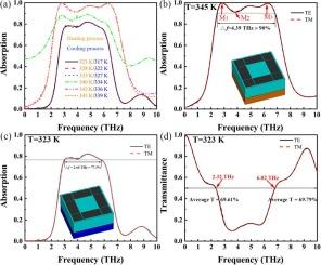
本文模拟并设计了一种由二氧化钒和石墨烯组成的经典三层结构比例太赫兹智能装置。这种智能器件的比例设置可以更好地控制表面微结构的尺寸,从而在生产过程中提高材料的利用率。在温度为 T = 345 K 时,该装置在 2.46 THz 至 6.85 THz(4.39 THz)的频率范围内表现出大于或等于 90 % 的完美吸收效率,几乎跨越了太赫兹波段的一半。在温度 T = 323 K 时,该器件在 3.04 THz 至 5.64 THz 频率范围内的吸收率超过 77.3%,在 0.01 THz 至 2.32 THz 和 6.82 THz 至 10.00 THz 频率范围内的平均透过率分别为 69.61% 和 69.79%。我们使用二氧化钒作为底层,以避免传统金属基底阻碍电磁波传输和限制太赫兹器件性能转换的影响。温度调制实现了对吸收和传输的控制。我们首先解释了基于 VO2 内部晶体结构的结果,然后利用表面等离子体(SP)分析了该器件在两个温度下的表面电场。通过调整吸收器的结构参数和施加外部偏置电压,可以改变石墨烯的费米能,从而证明了该器件的物理相干性、制造耐受性和动态调节能力。我们研究了外部电磁波不同入射角度对该器件性能的影响,结果表明它能在很大的角度范围内保持优异的性能,这对实际应用至关重要。最后,我们研究了在太赫兹范围内采用德鲁德模型表征二氧化硅的意义及其对器件性能的潜在影响。这对通信、探测、传感和成像具有重要意义,并为未来太赫兹器件的开发提供了启示。
本文章由计算机程序翻译,如有差异,请以英文原文为准。

Terahertz smart devices based on phase change material VO2 and metamaterial graphene that combine thermally adjustable absorption and selective transmission

Terahertz smart devices based on phase change material VO2 and metamaterial graphene that combine thermally adjustable absorption and selective transmission
In this paper, a classical three-layer structure of proportionate terahertz intelligent device composed of vanadium dioxide and graphene is simulated and designed. The proportionate setting of this intelligent device allows for better control over the size of surface microstructures, thereby enhancing the utilization of materials during the production process. At a temperature of T = 345 K, the device exhibits perfect absorption efficiency of greater than or equal to 90 % in the frequency range of 2.46 THz to 6.85 THz (4.39 THz), spanning almost half of the terahertz band. At a temperature of T = 323 K, the device achieves absorption of over 77.3 % in the frequency range of 3.04 THz to 5.64 THz, with average transmittance rates of 69.61 % and 69.79 % in the frequency ranges of 0.01 THz to 2.32 THz and 6.82 THz to 10.00 THz, respectively. We use vanadium dioxide as the bottom layer to avoid the effect of traditional metal substrates that prevent electromagnetic waves from transmitting and limit the conversion of terahertz device performance. Temperature modulation enables control over absorption and transmission. We first explain the results based on the crystal structure within VO2 and then analyze the surface electric field of the device at two temperatures using surface plasmons (SPs). By adjusting the structural parameters of the absorber and applying an external bias voltage, the Fermi energy of graphene can be altered, demonstrating the device’s physical coherence, manufacturing tolerance, and dynamic tuning capability. We investigate the influence of different incident angles of external electromagnetic waves on the device performance, showing that it maintains excellent performance over a wide range of angles, which is crucial for practical applications. Finally, we examined the implications of employing the Drude model to characterize silicon dioxide in the terahertz range and its potential impact on device performance. This holds significant implications for communication, detection, sensing, imaging, and provides insights for future terahertz device development.
求助全文
通过发布文献求助,成功后即可免费获取论文全文。 去求助
来源期刊
CiteScore
8.50
自引率
10.00%
发文量
1060
审稿时长
3.4 months
期刊介绍: Optics & Laser Technology aims to provide a vehicle for the publication of a broad range of high quality research and review papers in those fields of scientific and engineering research appertaining to the development and application of the technology of optics and lasers. Papers describing original work in these areas are submitted to rigorous refereeing prior to acceptance for publication. The scope of Optics & Laser Technology encompasses, but is not restricted to, the following areas: •development in all types of lasers •developments in optoelectronic devices and photonics •developments in new photonics and optical concepts •developments in conventional optics, optical instruments and components •techniques of optical metrology, including interferometry and optical fibre sensors •LIDAR and other non-contact optical measurement techniques, including optical methods in heat and fluid flow •applications of lasers to materials processing, optical NDT display (including holography) and optical communication •research and development in the field of laser safety including studies of hazards resulting from the applications of lasers (laser safety, hazards of laser fume) •developments in optical computing and optical information processing •developments in new optical materials •developments in new optical characterization methods and techniques •developments in quantum optics •developments in light assisted micro and nanofabrication methods and techniques •developments in nanophotonics and biophotonics •developments in imaging processing and systems
×
引用
GB/T 7714-2015
复制
MLA
复制
APA
复制
导出至
BibTeX EndNote RefMan NoteFirst NoteExpress
×
提示
您的信息不完整,为了账户安全,请先补充。
现在去补充
×
提示
您因"违规操作"
具体请查看互助需知
我知道了
×
提示
确定
请完成安全验证×
copy
已复制链接
快去分享给好友吧!
我知道了
右上角分享
点击右上角分享
0
联系我们:info@booksci.cn Book学术提供免费学术资源搜索服务,方便国内外学者检索中英文文献。致力于提供最便捷和优质的服务体验。 Copyright © 2023 布克学术 All rights reserved.
京ICP备2023020795号-1
ghs 京公网安备 11010802042870号
Book学术文献互助
Book学术文献互助群
群 号:481959085
Book学术官方微信