Arash Ghobadi, Cherian J. Mathai, Jacob Cook, Guang Bian, Salahuddin Attar, Mohammed Al-Hashimi, Shubhra Gangopadhyay, Suchismita Guha
{"title":"降低有机晶体管的势垒高度","authors":"Arash Ghobadi, Cherian J. Mathai, Jacob Cook, Guang Bian, Salahuddin Attar, Mohammed Al-Hashimi, Shubhra Gangopadhyay, Suchismita Guha","doi":"10.1002/aelm.202400503","DOIUrl":null,"url":null,"abstract":"<p>Reducing the Schottky barrier height and Fermi level de-pinning in metal-organic semiconductor contacts are crucial for enhancing the performance of organic transistors. The reduction of the Schottky barrier height in bottom-contact top-gate organic transistors is demonstrated by adding 1 nm thick atomic layer deposited Al<sub>2</sub>O<sub>3</sub> on the source and drain contacts. By using two different donor-acceptor copolymers, both <i>p-</i> and <i>n-</i>type transistors are investigated. Temperature-dependent current–voltage measurements from non-treated, self-assembled monolayer treated, and Al<sub>2</sub>O<sub>3</sub> treated Au source-drain contact field-effect transistors with varying channel lengths are carried out. The drain current versus drain voltage near zero gate voltage, which may be described by the thermionic emission model at temperatures above 150 K, allows the estimation of the Schottky barrier height (<i>φ<sub>B</sub></i>). The Al<sub>2</sub>O<sub>3</sub> contact-treated transistors show more than 40% lower <i>φ<sub>B</sub></i> compared with the non-treated contacts in the <i>p</i>-type transistor. Similarly, an isoindigo-based transistor, with <i>n</i>-type transport, shows a reduction in <i>φ<sub>B</sub></i> with Al<sub>2</sub>O<sub>3</sub> treated contacts suggesting that such ultrathin oxide layers provide a universal method for reducing the barrier height.</p>","PeriodicalId":110,"journal":{"name":"Advanced Electronic Materials","volume":"11 4","pages":""},"PeriodicalIF":5.3000,"publicationDate":"2024-10-04","publicationTypes":"Journal Article","fieldsOfStudy":null,"isOpenAccess":false,"openAccessPdf":"https://onlinelibrary.wiley.com/doi/epdf/10.1002/aelm.202400503","citationCount":"0","resultStr":"{\"title\":\"Reducing the Barrier Height in Organic Transistors\",\"authors\":\"Arash Ghobadi, Cherian J. Mathai, Jacob Cook, Guang Bian, Salahuddin Attar, Mohammed Al-Hashimi, Shubhra Gangopadhyay, Suchismita Guha\",\"doi\":\"10.1002/aelm.202400503\",\"DOIUrl\":null,\"url\":null,\"abstract\":\"<p>Reducing the Schottky barrier height and Fermi level de-pinning in metal-organic semiconductor contacts are crucial for enhancing the performance of organic transistors. The reduction of the Schottky barrier height in bottom-contact top-gate organic transistors is demonstrated by adding 1 nm thick atomic layer deposited Al<sub>2</sub>O<sub>3</sub> on the source and drain contacts. By using two different donor-acceptor copolymers, both <i>p-</i> and <i>n-</i>type transistors are investigated. Temperature-dependent current–voltage measurements from non-treated, self-assembled monolayer treated, and Al<sub>2</sub>O<sub>3</sub> treated Au source-drain contact field-effect transistors with varying channel lengths are carried out. The drain current versus drain voltage near zero gate voltage, which may be described by the thermionic emission model at temperatures above 150 K, allows the estimation of the Schottky barrier height (<i>φ<sub>B</sub></i>). The Al<sub>2</sub>O<sub>3</sub> contact-treated transistors show more than 40% lower <i>φ<sub>B</sub></i> compared with the non-treated contacts in the <i>p</i>-type transistor. Similarly, an isoindigo-based transistor, with <i>n</i>-type transport, shows a reduction in <i>φ<sub>B</sub></i> with Al<sub>2</sub>O<sub>3</sub> treated contacts suggesting that such ultrathin oxide layers provide a universal method for reducing the barrier height.</p>\",\"PeriodicalId\":110,\"journal\":{\"name\":\"Advanced Electronic Materials\",\"volume\":\"11 4\",\"pages\":\"\"},\"PeriodicalIF\":5.3000,\"publicationDate\":\"2024-10-04\",\"publicationTypes\":\"Journal Article\",\"fieldsOfStudy\":null,\"isOpenAccess\":false,\"openAccessPdf\":\"https://onlinelibrary.wiley.com/doi/epdf/10.1002/aelm.202400503\",\"citationCount\":\"0\",\"resultStr\":null,\"platform\":\"Semanticscholar\",\"paperid\":null,\"PeriodicalName\":\"Advanced Electronic Materials\",\"FirstCategoryId\":\"88\",\"ListUrlMain\":\"https://onlinelibrary.wiley.com/doi/10.1002/aelm.202400503\",\"RegionNum\":2,\"RegionCategory\":\"材料科学\",\"ArticlePicture\":[],\"TitleCN\":null,\"AbstractTextCN\":null,\"PMCID\":null,\"EPubDate\":\"\",\"PubModel\":\"\",\"JCR\":\"Q2\",\"JCRName\":\"MATERIALS SCIENCE, MULTIDISCIPLINARY\",\"Score\":null,\"Total\":0}","platform":"Semanticscholar","paperid":null,"PeriodicalName":"Advanced Electronic Materials","FirstCategoryId":"88","ListUrlMain":"https://onlinelibrary.wiley.com/doi/10.1002/aelm.202400503","RegionNum":2,"RegionCategory":"材料科学","ArticlePicture":[],"TitleCN":null,"AbstractTextCN":null,"PMCID":null,"EPubDate":"","PubModel":"","JCR":"Q2","JCRName":"MATERIALS SCIENCE, MULTIDISCIPLINARY","Score":null,"Total":0}
引用次数: 0
摘要
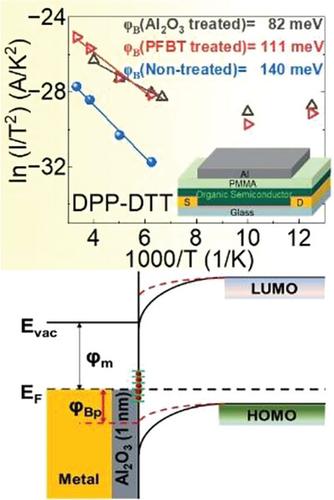
降低金属有机半导体触点的肖特基势垒高度和费米级去细化是提高有机晶体管性能的关键。通过在源极和漏极触点上添加 1 nm 厚的原子层沉积 Al2O3,降低了底部接触顶部栅极有机晶体管的肖特基势垒高度。通过使用两种不同的供体-受体共聚物,研究了 p 型和 n 型晶体管。对未经处理、经自组装单层处理和经 Al2O3 处理的具有不同沟道长度的金源漏接触场效应晶体管进行了随温度变化的电流电压测量。栅极电压为零附近的漏极电流与漏极电压的关系可以用温度高于 150 K 时的热离子发射模型来描述,从而可以估算出肖特基势垒高度 (φB)。经 Al2O3 触点处理的晶体管与未经处理的 p 型晶体管触点相比,φB 降低了 40% 以上。同样,经过 Al2O3 触点处理的异靛蓝基晶体管(具有 n 型传输)的φB 也有所降低,这表明这种超薄氧化物层提供了一种降低势垒高度的通用方法。
Reducing the Barrier Height in Organic Transistors
Reducing the Schottky barrier height and Fermi level de-pinning in metal-organic semiconductor contacts are crucial for enhancing the performance of organic transistors. The reduction of the Schottky barrier height in bottom-contact top-gate organic transistors is demonstrated by adding 1 nm thick atomic layer deposited Al2O3 on the source and drain contacts. By using two different donor-acceptor copolymers, both p- and n-type transistors are investigated. Temperature-dependent current–voltage measurements from non-treated, self-assembled monolayer treated, and Al2O3 treated Au source-drain contact field-effect transistors with varying channel lengths are carried out. The drain current versus drain voltage near zero gate voltage, which may be described by the thermionic emission model at temperatures above 150 K, allows the estimation of the Schottky barrier height (φB). The Al2O3 contact-treated transistors show more than 40% lower φB compared with the non-treated contacts in the p-type transistor. Similarly, an isoindigo-based transistor, with n-type transport, shows a reduction in φB with Al2O3 treated contacts suggesting that such ultrathin oxide layers provide a universal method for reducing the barrier height.
期刊介绍:
Advanced Electronic Materials is an interdisciplinary forum for peer-reviewed, high-quality, high-impact research in the fields of materials science, physics, and engineering of electronic and magnetic materials. It includes research on physics and physical properties of electronic and magnetic materials, spintronics, electronics, device physics and engineering, micro- and nano-electromechanical systems, and organic electronics, in addition to fundamental research.


 求助内容:
求助内容: 应助结果提醒方式:


