{"title":"高通量筛选二维材料,确定 p 型单层 WS2 为潜在的超高迁移率半导体","authors":"Viet-Anh Ha, Feliciano Giustino","doi":"10.1038/s41524-024-01417-0","DOIUrl":null,"url":null,"abstract":"<p>2D semiconductors offer a promising pathway to replace silicon in next-generation electronics. Among their many advantages, 2D materials possess atomically-sharp surfaces and enable scaling the channel thickness down to the monolayer limit. However, these materials exhibit comparatively lower charge carrier mobility and higher contact resistance than 3D semiconductors, making it challenging to realize high-performance devices at scale. In this work, we search for high-mobility 2D materials by combining a high-throughput screening strategy with state-of-the-art calculations based on the ab initio Boltzmann transport equation. Our analysis singles out a known transition metal dichalcogenide, monolayer WS<sub>2</sub>, as the most promising 2D semiconductor, with the potential to reach ultra-high room-temperature hole mobilities in excess of 1300 cm<sup>2</sup>/Vs should Ohmic contacts and low defect densities be achieved. Our work also highlights the importance of performing full-blown ab initio transport calculations to achieve predictive accuracy, including spin–orbital couplings, quasiparticle corrections, dipole and quadrupole long-range electron–phonon interactions, as well as scattering by point defects and extended defects.</p>","PeriodicalId":19342,"journal":{"name":"npj Computational Materials","volume":"1 1","pages":""},"PeriodicalIF":9.4000,"publicationDate":"2024-09-30","publicationTypes":"Journal Article","fieldsOfStudy":null,"isOpenAccess":false,"openAccessPdf":"","citationCount":"0","resultStr":"{\"title\":\"High-throughput screening of 2D materials identifies p-type monolayer WS2 as potential ultra-high mobility semiconductor\",\"authors\":\"Viet-Anh Ha, Feliciano Giustino\",\"doi\":\"10.1038/s41524-024-01417-0\",\"DOIUrl\":null,\"url\":null,\"abstract\":\"<p>2D semiconductors offer a promising pathway to replace silicon in next-generation electronics. Among their many advantages, 2D materials possess atomically-sharp surfaces and enable scaling the channel thickness down to the monolayer limit. However, these materials exhibit comparatively lower charge carrier mobility and higher contact resistance than 3D semiconductors, making it challenging to realize high-performance devices at scale. In this work, we search for high-mobility 2D materials by combining a high-throughput screening strategy with state-of-the-art calculations based on the ab initio Boltzmann transport equation. Our analysis singles out a known transition metal dichalcogenide, monolayer WS<sub>2</sub>, as the most promising 2D semiconductor, with the potential to reach ultra-high room-temperature hole mobilities in excess of 1300 cm<sup>2</sup>/Vs should Ohmic contacts and low defect densities be achieved. Our work also highlights the importance of performing full-blown ab initio transport calculations to achieve predictive accuracy, including spin–orbital couplings, quasiparticle corrections, dipole and quadrupole long-range electron–phonon interactions, as well as scattering by point defects and extended defects.</p>\",\"PeriodicalId\":19342,\"journal\":{\"name\":\"npj Computational Materials\",\"volume\":\"1 1\",\"pages\":\"\"},\"PeriodicalIF\":9.4000,\"publicationDate\":\"2024-09-30\",\"publicationTypes\":\"Journal Article\",\"fieldsOfStudy\":null,\"isOpenAccess\":false,\"openAccessPdf\":\"\",\"citationCount\":\"0\",\"resultStr\":null,\"platform\":\"Semanticscholar\",\"paperid\":null,\"PeriodicalName\":\"npj Computational Materials\",\"FirstCategoryId\":\"88\",\"ListUrlMain\":\"https://doi.org/10.1038/s41524-024-01417-0\",\"RegionNum\":1,\"RegionCategory\":\"材料科学\",\"ArticlePicture\":[],\"TitleCN\":null,\"AbstractTextCN\":null,\"PMCID\":null,\"EPubDate\":\"\",\"PubModel\":\"\",\"JCR\":\"Q1\",\"JCRName\":\"CHEMISTRY, PHYSICAL\",\"Score\":null,\"Total\":0}","platform":"Semanticscholar","paperid":null,"PeriodicalName":"npj Computational Materials","FirstCategoryId":"88","ListUrlMain":"https://doi.org/10.1038/s41524-024-01417-0","RegionNum":1,"RegionCategory":"材料科学","ArticlePicture":[],"TitleCN":null,"AbstractTextCN":null,"PMCID":null,"EPubDate":"","PubModel":"","JCR":"Q1","JCRName":"CHEMISTRY, PHYSICAL","Score":null,"Total":0}
引用次数: 0
摘要
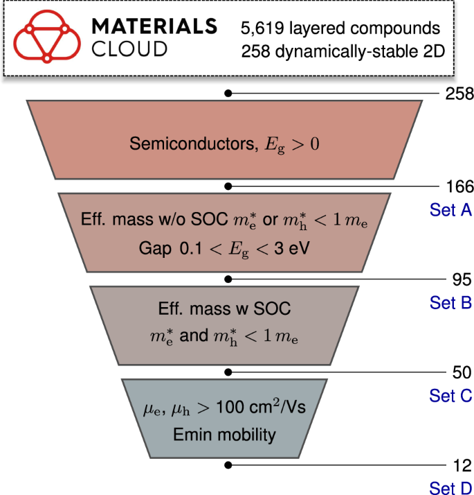
二维半导体为在下一代电子器件中取代硅提供了一条前景广阔的途径。二维材料具有许多优点,其中之一是拥有原子般锐利的表面,并能将沟道厚度缩减到单层极限。然而,与三维半导体相比,这些材料表现出较低的电荷载流子迁移率和较高的接触电阻,使得实现高性能器件的规模化具有挑战性。在这项研究中,我们将高通量筛选策略与基于非初始波尔兹曼输运方程的最新计算相结合,寻找高迁移率的二维材料。我们的分析发现,已知的过渡金属二掺杂物单层 WS2 是最有前途的二维半导体,如果实现欧姆接触和低缺陷密度,它有可能达到超过 1300 cm2/Vs 的超高室温空穴迁移率。我们的工作还强调了进行全面的 ab initio 传输计算以实现预测准确性的重要性,包括自旋轨道耦合、准粒子修正、偶极子和四极子长程电子-声子相互作用,以及点缺陷和扩展缺陷散射。
High-throughput screening of 2D materials identifies p-type monolayer WS2 as potential ultra-high mobility semiconductor
2D semiconductors offer a promising pathway to replace silicon in next-generation electronics. Among their many advantages, 2D materials possess atomically-sharp surfaces and enable scaling the channel thickness down to the monolayer limit. However, these materials exhibit comparatively lower charge carrier mobility and higher contact resistance than 3D semiconductors, making it challenging to realize high-performance devices at scale. In this work, we search for high-mobility 2D materials by combining a high-throughput screening strategy with state-of-the-art calculations based on the ab initio Boltzmann transport equation. Our analysis singles out a known transition metal dichalcogenide, monolayer WS2, as the most promising 2D semiconductor, with the potential to reach ultra-high room-temperature hole mobilities in excess of 1300 cm2/Vs should Ohmic contacts and low defect densities be achieved. Our work also highlights the importance of performing full-blown ab initio transport calculations to achieve predictive accuracy, including spin–orbital couplings, quasiparticle corrections, dipole and quadrupole long-range electron–phonon interactions, as well as scattering by point defects and extended defects.
期刊介绍:
npj Computational Materials is a high-quality open access journal from Nature Research that publishes research papers applying computational approaches for the design of new materials and enhancing our understanding of existing ones. The journal also welcomes papers on new computational techniques and the refinement of current approaches that support these aims, as well as experimental papers that complement computational findings.
Some key features of npj Computational Materials include a 2-year impact factor of 12.241 (2021), article downloads of 1,138,590 (2021), and a fast turnaround time of 11 days from submission to the first editorial decision. The journal is indexed in various databases and services, including Chemical Abstracts Service (ACS), Astrophysics Data System (ADS), Current Contents/Physical, Chemical and Earth Sciences, Journal Citation Reports/Science Edition, SCOPUS, EI Compendex, INSPEC, Google Scholar, SCImago, DOAJ, CNKI, and Science Citation Index Expanded (SCIE), among others.
 求助内容:
求助内容: 应助结果提醒方式:


