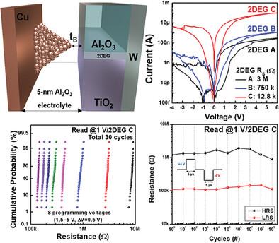
利用二维电子气体实现具有可调隧道间隙和更佳开关均匀性的垂直开关导电桥式随机存取存储器

IF 5.3 2区 材料科学 Q2 MATERIALS SCIENCE, MULTIDISCIPLINARY
Jiho Kim, Ohhyuk Kwon, Jongseon Seo, Hyunsang Hwang
{"title":"利用二维电子气体实现具有可调隧道间隙和更佳开关均匀性的垂直开关导电桥式随机存取存储器","authors":"Jiho Kim, Ohhyuk Kwon, Jongseon Seo, Hyunsang Hwang","doi":"10.1002/aelm.202400650","DOIUrl":null,"url":null,"abstract":"Owing to the high reactivity and diffusivity of Ag and Cu ions, controlling the atomic filament formation and rupture processes in conductive bridge random-access memory (CBRAM) is challenging. In this study, it is demonstrated that by using a 2D electron gas (2DEG) as the bottom electrode (BE) in a vertical-switching CBRAM (V-CBRAM), filament formation and rupture can be effectively managed and the tunnel gap distance created by partial filament formation can be adjusted. The 2DEG BE induces partial filament formation by limiting the number of electrons required for this process in the V-CBRAM device, as verified via current fitting to the quantum point contact model. Varying the electron concentration and activation energy for electrons trapped in the 2DEG, when paired with various programming voltages, leads to transitions in the device resistance state via changes in the distance of the tunnel gap. This tunnel-gap-tunable 2DEG V-CBRAM device, which exhibits superior switching uniformity, can be employed for nonvolatile memory applications in the sub-G<sub>0</sub> conductance regime, such as 3-bit multilevel cells and selector-less memory.","PeriodicalId":110,"journal":{"name":"Advanced Electronic Materials","volume":"38 1","pages":""},"PeriodicalIF":5.3000,"publicationDate":"2024-09-18","publicationTypes":"Journal Article","fieldsOfStudy":null,"isOpenAccess":false,"openAccessPdf":"","citationCount":"0","resultStr":"{\"title\":\"Vertical-Switching Conductive Bridge Random Access Memory with Adjustable Tunnel Gap and Improved Switching Uniformity Using 2D Electron Gas\",\"authors\":\"Jiho Kim, Ohhyuk Kwon, Jongseon Seo, Hyunsang Hwang\",\"doi\":\"10.1002/aelm.202400650\",\"DOIUrl\":null,\"url\":null,\"abstract\":\"Owing to the high reactivity and diffusivity of Ag and Cu ions, controlling the atomic filament formation and rupture processes in conductive bridge random-access memory (CBRAM) is challenging. In this study, it is demonstrated that by using a 2D electron gas (2DEG) as the bottom electrode (BE) in a vertical-switching CBRAM (V-CBRAM), filament formation and rupture can be effectively managed and the tunnel gap distance created by partial filament formation can be adjusted. The 2DEG BE induces partial filament formation by limiting the number of electrons required for this process in the V-CBRAM device, as verified via current fitting to the quantum point contact model. Varying the electron concentration and activation energy for electrons trapped in the 2DEG, when paired with various programming voltages, leads to transitions in the device resistance state via changes in the distance of the tunnel gap. This tunnel-gap-tunable 2DEG V-CBRAM device, which exhibits superior switching uniformity, can be employed for nonvolatile memory applications in the sub-G<sub>0</sub> conductance regime, such as 3-bit multilevel cells and selector-less memory.\",\"PeriodicalId\":110,\"journal\":{\"name\":\"Advanced Electronic Materials\",\"volume\":\"38 1\",\"pages\":\"\"},\"PeriodicalIF\":5.3000,\"publicationDate\":\"2024-09-18\",\"publicationTypes\":\"Journal Article\",\"fieldsOfStudy\":null,\"isOpenAccess\":false,\"openAccessPdf\":\"\",\"citationCount\":\"0\",\"resultStr\":null,\"platform\":\"Semanticscholar\",\"paperid\":null,\"PeriodicalName\":\"Advanced Electronic Materials\",\"FirstCategoryId\":\"88\",\"ListUrlMain\":\"https://doi.org/10.1002/aelm.202400650\",\"RegionNum\":2,\"RegionCategory\":\"材料科学\",\"ArticlePicture\":[],\"TitleCN\":null,\"AbstractTextCN\":null,\"PMCID\":null,\"EPubDate\":\"\",\"PubModel\":\"\",\"JCR\":\"Q2\",\"JCRName\":\"MATERIALS SCIENCE, MULTIDISCIPLINARY\",\"Score\":null,\"Total\":0}","platform":"Semanticscholar","paperid":null,"PeriodicalName":"Advanced Electronic Materials","FirstCategoryId":"88","ListUrlMain":"https://doi.org/10.1002/aelm.202400650","RegionNum":2,"RegionCategory":"材料科学","ArticlePicture":[],"TitleCN":null,"AbstractTextCN":null,"PMCID":null,"EPubDate":"","PubModel":"","JCR":"Q2","JCRName":"MATERIALS SCIENCE, MULTIDISCIPLINARY","Score":null,"Total":0}
引用次数: 0

摘要

由于银离子和铜离子的高反应性和高扩散性,在导电桥式随机存取存储器(CBRAM)中控制原子丝的形成和断裂过程具有挑战性。本研究证明,在垂直开关式 CBRAM(V-CBRAM)中使用二维电子气体(2DEG)作为底电极(BE),可以有效地控制灯丝的形成和断裂,并且可以调整部分灯丝形成所产生的隧道间隙距离。通过量子点接触模型的电流拟合验证,2DEG BE 可以通过限制 V-CBRAM 器件中这一过程所需的电子数量来诱导部分灯丝的形成。在各种编程电压的配合下,改变二维电子元件中电子的浓度和活化能,就能通过隧道间隙距离的变化实现器件电阻状态的转变。这种隧道间隙可调的 2DEG V-CBRAM 器件具有出色的开关均匀性,可应用于亚 G0 电导机制下的非易失性存储器应用,如 3 位多层电池和无选择器存储器。
本文章由计算机程序翻译,如有差异,请以英文原文为准。

Vertical-Switching Conductive Bridge Random Access Memory with Adjustable Tunnel Gap and Improved Switching Uniformity Using 2D Electron Gas

Vertical-Switching Conductive Bridge Random Access Memory with Adjustable Tunnel Gap and Improved Switching Uniformity Using 2D Electron Gas
Owing to the high reactivity and diffusivity of Ag and Cu ions, controlling the atomic filament formation and rupture processes in conductive bridge random-access memory (CBRAM) is challenging. In this study, it is demonstrated that by using a 2D electron gas (2DEG) as the bottom electrode (BE) in a vertical-switching CBRAM (V-CBRAM), filament formation and rupture can be effectively managed and the tunnel gap distance created by partial filament formation can be adjusted. The 2DEG BE induces partial filament formation by limiting the number of electrons required for this process in the V-CBRAM device, as verified via current fitting to the quantum point contact model. Varying the electron concentration and activation energy for electrons trapped in the 2DEG, when paired with various programming voltages, leads to transitions in the device resistance state via changes in the distance of the tunnel gap. This tunnel-gap-tunable 2DEG V-CBRAM device, which exhibits superior switching uniformity, can be employed for nonvolatile memory applications in the sub-G0 conductance regime, such as 3-bit multilevel cells and selector-less memory.
求助全文
通过发布文献求助,成功后即可免费获取论文全文。 去求助
来源期刊
Advanced Electronic Materials
Advanced Electronic Materials NANOSCIENCE & NANOTECHNOLOGYMATERIALS SCIE-MATERIALS SCIENCE, MULTIDISCIPLINARY
CiteScore
11.00
自引率
3.20%
发文量
433
期刊介绍: Advanced Electronic Materials is an interdisciplinary forum for peer-reviewed, high-quality, high-impact research in the fields of materials science, physics, and engineering of electronic and magnetic materials. It includes research on physics and physical properties of electronic and magnetic materials, spintronics, electronics, device physics and engineering, micro- and nano-electromechanical systems, and organic electronics, in addition to fundamental research.
×
引用
GB/T 7714-2015
复制
MLA
复制
APA
复制
导出至
BibTeX EndNote RefMan NoteFirst NoteExpress
×
提示
您的信息不完整,为了账户安全,请先补充。
现在去补充
×
提示
您因"违规操作"
具体请查看互助需知
我知道了
×
提示
确定
请完成安全验证×
copy
已复制链接
快去分享给好友吧!
我知道了
右上角分享
点击右上角分享
0
联系我们:info@booksci.cn Book学术提供免费学术资源搜索服务,方便国内外学者检索中英文文献。致力于提供最便捷和优质的服务体验。 Copyright © 2023 布克学术 All rights reserved.
京ICP备2023020795号-1
ghs 京公网安备 11010802042870号
Book学术文献互助
Book学术文献互助群
群 号:481959085
Book学术官方微信