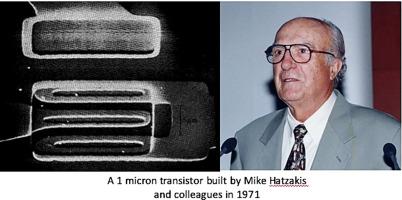
迈克尔-哈扎基斯,半导体行业先驱

IF 2.8 Q2 ENGINEERING, ELECTRICAL & ELECTRONIC
J. Paraszczak , J.M. Shaw , D.P. Kern , P. Argitis , D. Davazoglou , I. Raptis , D. Tsoukalas , E. Gogolides
{"title":"迈克尔-哈扎基斯,半导体行业先驱","authors":"J. Paraszczak ,&nbsp;J.M. Shaw ,&nbsp;D.P. Kern ,&nbsp;P. Argitis ,&nbsp;D. Davazoglou ,&nbsp;I. Raptis ,&nbsp;D. Tsoukalas ,&nbsp;E. Gogolides","doi":"10.1016/j.mne.2024.100276","DOIUrl":null,"url":null,"abstract":"<div><p>Although this opinion paper tracks the career of Mike Hatzakis (as he liked to be called), and explains the impact he made on the IT industry, it is not intended to be comprehensive insofar as the work that was underway during his career is concerned. Thus, the intent is not to cite all relevant work in the field of Semiconductor lithography, where Mike made such an impact, but to provide a historic and human perspective of this remarkable man from the land of the Minotaur (Crete) and his career, the work he championed in his labs in the US and later Greece and his very human approach to science, technology, and to people.<span><figure><span><img><ol><li><span><span>Download: <span>Download high-res image (200KB)</span></span></span></li><li><span><span>Download: <span>Download full-size image</span></span></span></li></ol></span></figure></span></p></div>","PeriodicalId":37111,"journal":{"name":"Micro and Nano Engineering","volume":"24 ","pages":"Article 100276"},"PeriodicalIF":2.8000,"publicationDate":"2024-07-27","publicationTypes":"Journal Article","fieldsOfStudy":null,"isOpenAccess":false,"openAccessPdf":"https://www.sciencedirect.com/science/article/pii/S259000722400039X/pdfft?md5=0dd817c39162f110bd05b18c50bfab77&pid=1-s2.0-S259000722400039X-main.pdf","citationCount":"0","resultStr":"{\"title\":\"Michael Hatzakis, semiconductor industry pioneer\",\"authors\":\"J. Paraszczak ,&nbsp;J.M. Shaw ,&nbsp;D.P. Kern ,&nbsp;P. Argitis ,&nbsp;D. Davazoglou ,&nbsp;I. Raptis ,&nbsp;D. Tsoukalas ,&nbsp;E. Gogolides\",\"doi\":\"10.1016/j.mne.2024.100276\",\"DOIUrl\":null,\"url\":null,\"abstract\":\"<div><p>Although this opinion paper tracks the career of Mike Hatzakis (as he liked to be called), and explains the impact he made on the IT industry, it is not intended to be comprehensive insofar as the work that was underway during his career is concerned. Thus, the intent is not to cite all relevant work in the field of Semiconductor lithography, where Mike made such an impact, but to provide a historic and human perspective of this remarkable man from the land of the Minotaur (Crete) and his career, the work he championed in his labs in the US and later Greece and his very human approach to science, technology, and to people.<span><figure><span><img><ol><li><span><span>Download: <span>Download high-res image (200KB)</span></span></span></li><li><span><span>Download: <span>Download full-size image</span></span></span></li></ol></span></figure></span></p></div>\",\"PeriodicalId\":37111,\"journal\":{\"name\":\"Micro and Nano Engineering\",\"volume\":\"24 \",\"pages\":\"Article 100276\"},\"PeriodicalIF\":2.8000,\"publicationDate\":\"2024-07-27\",\"publicationTypes\":\"Journal Article\",\"fieldsOfStudy\":null,\"isOpenAccess\":false,\"openAccessPdf\":\"https://www.sciencedirect.com/science/article/pii/S259000722400039X/pdfft?md5=0dd817c39162f110bd05b18c50bfab77&pid=1-s2.0-S259000722400039X-main.pdf\",\"citationCount\":\"0\",\"resultStr\":null,\"platform\":\"Semanticscholar\",\"paperid\":null,\"PeriodicalName\":\"Micro and Nano Engineering\",\"FirstCategoryId\":\"1085\",\"ListUrlMain\":\"https://www.sciencedirect.com/science/article/pii/S259000722400039X\",\"RegionNum\":0,\"RegionCategory\":null,\"ArticlePicture\":[],\"TitleCN\":null,\"AbstractTextCN\":null,\"PMCID\":null,\"EPubDate\":\"\",\"PubModel\":\"\",\"JCR\":\"Q2\",\"JCRName\":\"ENGINEERING, ELECTRICAL & ELECTRONIC\",\"Score\":null,\"Total\":0}","platform":"Semanticscholar","paperid":null,"PeriodicalName":"Micro and Nano Engineering","FirstCategoryId":"1085","ListUrlMain":"https://www.sciencedirect.com/science/article/pii/S259000722400039X","RegionNum":0,"RegionCategory":null,"ArticlePicture":[],"TitleCN":null,"AbstractTextCN":null,"PMCID":null,"EPubDate":"","PubModel":"","JCR":"Q2","JCRName":"ENGINEERING, ELECTRICAL & ELECTRONIC","Score":null,"Total":0}
引用次数: 0

摘要

尽管本意见书追溯了迈克-哈扎基斯(Mike Hatzakis,人们喜欢这样称呼他)的职业生涯,并解释了他对 IT 行业的影响,但就其职业生涯中正在进行的工作而言,本意见书并不打算做到面面俱到。因此,本书的目的并不是列举迈克在半导体光刻领域所做的所有相关工作,而是从历史和人性的角度,介绍这位来自牛头人之乡(克里特岛)的杰出人物及其职业生涯、他在美国和希腊实验室所倡导的工作,以及他对科学、技术和人所采取的非常人性化的方法:下载高清图片 (200KB)Download:下载全尺寸图片
本文章由计算机程序翻译,如有差异,请以英文原文为准。

Michael Hatzakis, semiconductor industry pioneer

Michael Hatzakis, semiconductor industry pioneer

Although this opinion paper tracks the career of Mike Hatzakis (as he liked to be called), and explains the impact he made on the IT industry, it is not intended to be comprehensive insofar as the work that was underway during his career is concerned. Thus, the intent is not to cite all relevant work in the field of Semiconductor lithography, where Mike made such an impact, but to provide a historic and human perspective of this remarkable man from the land of the Minotaur (Crete) and his career, the work he championed in his labs in the US and later Greece and his very human approach to science, technology, and to people.

  1. Download: Download high-res image (200KB)
  2. Download: Download full-size image

求助全文
通过发布文献求助,成功后即可免费获取论文全文。 去求助
来源期刊
Micro and Nano Engineering
Micro and Nano Engineering Engineering-Electrical and Electronic Engineering
CiteScore
3.30
自引率
0.00%
发文量
67
审稿时长
80 days
×
引用
GB/T 7714-2015
复制
MLA
复制
APA
复制
导出至
BibTeX EndNote RefMan NoteFirst NoteExpress
×
提示
您的信息不完整,为了账户安全,请先补充。
现在去补充
×
提示
您因"违规操作"
具体请查看互助需知
我知道了
×
提示
确定
请完成安全验证×
copy
已复制链接
快去分享给好友吧!
我知道了
右上角分享
点击右上角分享
0
联系我们:info@booksci.cn Book学术提供免费学术资源搜索服务,方便国内外学者检索中英文文献。致力于提供最便捷和优质的服务体验。 Copyright © 2023 布克学术 All rights reserved.
京ICP备2023020795号-1
ghs 京公网安备 11010802042870号
Book学术文献互助
Book学术文献互助群
群 号:481959085
Book学术官方微信