超级闪存非易失性存储器单元的结构与形成

Q4 Engineering
D. A. Abdullaev, E. V. Bobrova, R. A. Milovanov
{"title":"超级闪存非易失性存储器单元的结构与形成","authors":"D. A. Abdullaev, E. V. Bobrova, R. A. Milovanov","doi":"10.1134/s1063739724600249","DOIUrl":null,"url":null,"abstract":"<h3 data-test=\"abstract-sub-heading\">Abstract</h3><p>Split-gate embedded Flash memory technology has been around for decades and has become the standard application for a wide range of devices such as microcontrollers and smart cards. Among them, due to a number of advantages, SuperFlash (SF) produced by Silicon Storage Technology is the most widely used nonvolatile memory technology. In this paper, the results of a study of the structure of memory cells (MCs) are presented and the principle of their operation, as well as the main technological stages of the production process of forming transistor structures, is discussed.</p>","PeriodicalId":21534,"journal":{"name":"Russian Microelectronics","volume":"53 1","pages":""},"PeriodicalIF":0.0000,"publicationDate":"2024-07-26","publicationTypes":"Journal Article","fieldsOfStudy":null,"isOpenAccess":false,"openAccessPdf":"","citationCount":"0","resultStr":"{\"title\":\"Structure and Formation of Superflash Nonvolatile Memory Cells\",\"authors\":\"D. A. Abdullaev, E. V. Bobrova, R. A. Milovanov\",\"doi\":\"10.1134/s1063739724600249\",\"DOIUrl\":null,\"url\":null,\"abstract\":\"<h3 data-test=\\\"abstract-sub-heading\\\">Abstract</h3><p>Split-gate embedded Flash memory technology has been around for decades and has become the standard application for a wide range of devices such as microcontrollers and smart cards. Among them, due to a number of advantages, SuperFlash (SF) produced by Silicon Storage Technology is the most widely used nonvolatile memory technology. In this paper, the results of a study of the structure of memory cells (MCs) are presented and the principle of their operation, as well as the main technological stages of the production process of forming transistor structures, is discussed.</p>\",\"PeriodicalId\":21534,\"journal\":{\"name\":\"Russian Microelectronics\",\"volume\":\"53 1\",\"pages\":\"\"},\"PeriodicalIF\":0.0000,\"publicationDate\":\"2024-07-26\",\"publicationTypes\":\"Journal Article\",\"fieldsOfStudy\":null,\"isOpenAccess\":false,\"openAccessPdf\":\"\",\"citationCount\":\"0\",\"resultStr\":null,\"platform\":\"Semanticscholar\",\"paperid\":null,\"PeriodicalName\":\"Russian Microelectronics\",\"FirstCategoryId\":\"1085\",\"ListUrlMain\":\"https://doi.org/10.1134/s1063739724600249\",\"RegionNum\":0,\"RegionCategory\":null,\"ArticlePicture\":[],\"TitleCN\":null,\"AbstractTextCN\":null,\"PMCID\":null,\"EPubDate\":\"\",\"PubModel\":\"\",\"JCR\":\"Q4\",\"JCRName\":\"Engineering\",\"Score\":null,\"Total\":0}","platform":"Semanticscholar","paperid":null,"PeriodicalName":"Russian Microelectronics","FirstCategoryId":"1085","ListUrlMain":"https://doi.org/10.1134/s1063739724600249","RegionNum":0,"RegionCategory":null,"ArticlePicture":[],"TitleCN":null,"AbstractTextCN":null,"PMCID":null,"EPubDate":"","PubModel":"","JCR":"Q4","JCRName":"Engineering","Score":null,"Total":0}
引用次数: 0

摘要

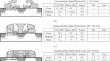
摘要分路栅极嵌入式闪存技术已有几十年的历史,已成为微控制器和智能卡等多种设备的标准应用。其中,硅存储技术公司(Silicon Storage Technology)生产的超级闪存(SuperFlash,SF)因其诸多优点而成为应用最广泛的非易失性存储器技术。本文介绍了存储单元(MC)结构的研究成果,并讨论了其工作原理以及形成晶体管结构的生产过程的主要技术阶段。
本文章由计算机程序翻译,如有差异,请以英文原文为准。

Structure and Formation of Superflash Nonvolatile Memory Cells

Structure and Formation of Superflash Nonvolatile Memory Cells

Abstract

Split-gate embedded Flash memory technology has been around for decades and has become the standard application for a wide range of devices such as microcontrollers and smart cards. Among them, due to a number of advantages, SuperFlash (SF) produced by Silicon Storage Technology is the most widely used nonvolatile memory technology. In this paper, the results of a study of the structure of memory cells (MCs) are presented and the principle of their operation, as well as the main technological stages of the production process of forming transistor structures, is discussed.

求助全文
通过发布文献求助,成功后即可免费获取论文全文。 去求助
来源期刊
Russian Microelectronics
Russian Microelectronics Materials Science-Materials Chemistry
CiteScore
0.70
自引率
0.00%
发文量
43
期刊介绍: Russian Microelectronics  covers physical, technological, and some VLSI and ULSI circuit-technical aspects of microelectronics and nanoelectronics; it informs the reader of new trends in submicron optical, x-ray, electron, and ion-beam lithography technology; dry processing techniques, etching, doping; and deposition and planarization technology. Significant space is devoted to problems arising in the application of proton, electron, and ion beams, plasma, etc. Consideration is given to new equipment, including cluster tools and control in situ and submicron CMOS, bipolar, and BICMOS technologies. The journal publishes papers addressing problems of molecular beam epitaxy and related processes; heterojunction devices and integrated circuits; the technology and devices of nanoelectronics; and the fabrication of nanometer scale devices, including new device structures, quantum-effect devices, and superconducting devices. The reader will find papers containing news of the diagnostics of surfaces and microelectronic structures, the modeling of technological processes and devices in micro- and nanoelectronics, including nanotransistors, and solid state qubits.
×
引用
GB/T 7714-2015
复制
MLA
复制
APA
复制
导出至
BibTeX EndNote RefMan NoteFirst NoteExpress
×
提示
您的信息不完整,为了账户安全,请先补充。
现在去补充
×
提示
您因"违规操作"
具体请查看互助需知
我知道了
×
提示
确定
请完成安全验证×
copy
已复制链接
快去分享给好友吧!
我知道了
右上角分享
点击右上角分享
0
联系我们:info@booksci.cn Book学术提供免费学术资源搜索服务,方便国内外学者检索中英文文献。致力于提供最便捷和优质的服务体验。 Copyright © 2023 布克学术 All rights reserved.
京ICP备2023020795号-1
ghs 京公网安备 11010802042870号
Book学术文献互助
Book学术文献互助群
群 号:604180095
Book学术官方微信