基于范德华 MoS2/MoTe2 异质双电层的红外线光电探测器
IF 5.3
2区 材料科学
Q2 MATERIALS SCIENCE, MULTIDISCIPLINARY
引用次数: 0
摘要
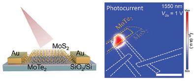
基于二维异质层的光电探测器可以克服单个二维单层的带隙限制,在相对较长的波长下工作。然而,异质层内超低的光吸收率会导致极弱的光致发光性。在这里,基于 MoS2/MoTe2 II 型异质双分子层的红外光探测器在 1550 纳米波长处的光致发光率达到了 0.55 A W-1,远远超过了单层 MoS2 和 MoTe2 的能带截止点,这主要是光ogating 效应的结果。拉曼光谱和光致发光(PL)光谱揭示了异质双电层中强烈的层间耦合,并在 1550 纳米附近观察到一个宽的 PL 峰,该峰值归因于载流子的层间跃迁。光电探测器具有从 1100 纳米到 1700 纳米的宽带检测能力,其中 1550 纳米处的峰值与层间吸收相对应。基于异质层的场效应晶体管的电学特性分析和开尔文探针力显微镜显示了高效的层间空穴传输。反应灵敏的 MoS2/MoTe2 红外光探测器具有≈103 的大光电增益和 130 毫秒的时间常数。这项研究揭示了层间跃迁如何影响基于二维异质层的光电探测器,并推动了层状半导体异质结构的利用。本文章由计算机程序翻译,如有差异,请以英文原文为准。
Infrared Photodetector Based on van der Waals MoS2/MoTe2 Hetero-Bilayer Modulated by Photogating
Photodetectors based on 2D hetero-bilayers can overcome the bandgap limitations of individual 2D monolayers and operate at relatively long wavelengths. However, ultra-low light absorptions within hetero-bilayers result in extremely weak photoresponsivity. Here, an infrared photodetector based on the MoS2/MoTe2 type-II hetero-bilayer is demonstrated to reach a photoresponsivity of 0.55 A W−1 at 1550 nm, well beyond energy band cut-offs of monolayer MoS2 and MoTe2, primarily resulted from the photogating effect. Raman and photoluminescence (PL) spectroscopy reveal strong interlayer couplings in the hetero-bilayer, and a broad PL peak around 1550 nm is observed that is ascribed to interlayer transitions of carriers. The photodetector showcases a broadband detection capability from 1100 to 1700 nm, with a peak at 1550 nm corresponding to the interlayer absorption. Electrical characterization of the hetero-bilayer-based field-effect transistor and kelvin probe force microscopy reveal efficient interlayer hole transfer. The highly responsive MoS2/MoTe2 infrared photodetector offers a large photo-gain of ≈103 and a time constant of 130 ms. The research illuminates how interlayer transitions affect 2D hetero-bilayer-based photodetectors and advances the utilization of layered semiconductor heterostructures.
求助全文
通过发布文献求助,成功后即可免费获取论文全文。
去求助
来源期刊
Advanced Electronic Materials
NANOSCIENCE & NANOTECHNOLOGYMATERIALS SCIE-MATERIALS SCIENCE, MULTIDISCIPLINARY
CiteScore
11.00
自引率
3.20%
发文量
433
期刊介绍:
Advanced Electronic Materials is an interdisciplinary forum for peer-reviewed, high-quality, high-impact research in the fields of materials science, physics, and engineering of electronic and magnetic materials. It includes research on physics and physical properties of electronic and magnetic materials, spintronics, electronics, device physics and engineering, micro- and nano-electromechanical systems, and organic electronics, in addition to fundamental research.
 求助内容:
求助内容: 应助结果提醒方式:


