Maksym Myronov, Pedram Jahandar, Simone Rossi, Kevin Sewell, Felipe Murphy-Armando, Fabio Pezzoli
{"title":"在异常低温条件下高效原位掺杂应变锗锡外延层","authors":"Maksym Myronov, Pedram Jahandar, Simone Rossi, Kevin Sewell, Felipe Murphy-Armando, Fabio Pezzoli","doi":"10.1002/aelm.202300811","DOIUrl":null,"url":null,"abstract":"<p>Efficient p- and n-type in situ doping of compressively strained germanium tin (Ge<sub>1-x</sub>Sn<sub>x</sub>) semiconductor epilayers, grown by chemical vapor deposition on a standard Si(001) substrate, is demonstrated. Materials characterization results reveal unusual impact of dopants manifesting via a pronounced reduction of Sn content in the epilayer, accompanied by an enhancement of the growth rate, due to increasing p-type doping concentration. Furthermore, the opposite behavior for n-type doping is observed, resulting in a less pronounced increase of Sn concentration and no effect on growth rate. Nevertheless, a very high density of electrically active holes up to ≈4 × 10<sup>20</sup> cm<sup>−3</sup> is obtained in p-type doped Ge<sub>1-x</sub>Sn<sub>x</sub> epilayer resulting in the lowest resistivity of 0.15 mΩ cm among all in situ doped epitaxial and strained group-IV semiconductors. Also, the metal-to-insulator transition in Ge<sub>1-x</sub>Sn<sub>x</sub> is experimentally demonstrated for doping levels above 1 × 10<sup>17</sup> cm<sup>−3</sup>, which is substantially lower than in any group-IV semiconductor, and theoretically predict it to be as low as ≈1 × 10<sup>17</sup> cm<sup>−3</sup>. The findings enabled by the doping regime explored in this work can open novel prospects to engineer low resistivity contacts and charge current injection in applications covering next-generation transistors, qubits, diodes, electrically driven light sources, sensors and hybrid quantum devices.</p>","PeriodicalId":110,"journal":{"name":"Advanced Electronic Materials","volume":null,"pages":null},"PeriodicalIF":5.3000,"publicationDate":"2024-07-02","publicationTypes":"Journal Article","fieldsOfStudy":null,"isOpenAccess":false,"openAccessPdf":"https://onlinelibrary.wiley.com/doi/epdf/10.1002/aelm.202300811","citationCount":"0","resultStr":"{\"title\":\"Efficient In Situ Doping of Strained Germanium Tin Epilayers at Unusually Low Temperature\",\"authors\":\"Maksym Myronov, Pedram Jahandar, Simone Rossi, Kevin Sewell, Felipe Murphy-Armando, Fabio Pezzoli\",\"doi\":\"10.1002/aelm.202300811\",\"DOIUrl\":null,\"url\":null,\"abstract\":\"<p>Efficient p- and n-type in situ doping of compressively strained germanium tin (Ge<sub>1-x</sub>Sn<sub>x</sub>) semiconductor epilayers, grown by chemical vapor deposition on a standard Si(001) substrate, is demonstrated. Materials characterization results reveal unusual impact of dopants manifesting via a pronounced reduction of Sn content in the epilayer, accompanied by an enhancement of the growth rate, due to increasing p-type doping concentration. Furthermore, the opposite behavior for n-type doping is observed, resulting in a less pronounced increase of Sn concentration and no effect on growth rate. Nevertheless, a very high density of electrically active holes up to ≈4 × 10<sup>20</sup> cm<sup>−3</sup> is obtained in p-type doped Ge<sub>1-x</sub>Sn<sub>x</sub> epilayer resulting in the lowest resistivity of 0.15 mΩ cm among all in situ doped epitaxial and strained group-IV semiconductors. Also, the metal-to-insulator transition in Ge<sub>1-x</sub>Sn<sub>x</sub> is experimentally demonstrated for doping levels above 1 × 10<sup>17</sup> cm<sup>−3</sup>, which is substantially lower than in any group-IV semiconductor, and theoretically predict it to be as low as ≈1 × 10<sup>17</sup> cm<sup>−3</sup>. The findings enabled by the doping regime explored in this work can open novel prospects to engineer low resistivity contacts and charge current injection in applications covering next-generation transistors, qubits, diodes, electrically driven light sources, sensors and hybrid quantum devices.</p>\",\"PeriodicalId\":110,\"journal\":{\"name\":\"Advanced Electronic Materials\",\"volume\":null,\"pages\":null},\"PeriodicalIF\":5.3000,\"publicationDate\":\"2024-07-02\",\"publicationTypes\":\"Journal Article\",\"fieldsOfStudy\":null,\"isOpenAccess\":false,\"openAccessPdf\":\"https://onlinelibrary.wiley.com/doi/epdf/10.1002/aelm.202300811\",\"citationCount\":\"0\",\"resultStr\":null,\"platform\":\"Semanticscholar\",\"paperid\":null,\"PeriodicalName\":\"Advanced Electronic Materials\",\"FirstCategoryId\":\"88\",\"ListUrlMain\":\"https://onlinelibrary.wiley.com/doi/10.1002/aelm.202300811\",\"RegionNum\":2,\"RegionCategory\":\"材料科学\",\"ArticlePicture\":[],\"TitleCN\":null,\"AbstractTextCN\":null,\"PMCID\":null,\"EPubDate\":\"\",\"PubModel\":\"\",\"JCR\":\"Q2\",\"JCRName\":\"MATERIALS SCIENCE, MULTIDISCIPLINARY\",\"Score\":null,\"Total\":0}","platform":"Semanticscholar","paperid":null,"PeriodicalName":"Advanced Electronic Materials","FirstCategoryId":"88","ListUrlMain":"https://onlinelibrary.wiley.com/doi/10.1002/aelm.202300811","RegionNum":2,"RegionCategory":"材料科学","ArticlePicture":[],"TitleCN":null,"AbstractTextCN":null,"PMCID":null,"EPubDate":"","PubModel":"","JCR":"Q2","JCRName":"MATERIALS SCIENCE, MULTIDISCIPLINARY","Score":null,"Total":0}
引用次数: 0
摘要
通过化学气相沉积法在标准硅(001)衬底上生长出的压缩应变锗锡(Ge1-xSnx)半导体外延层中进行了高效的 p 型和 n 型原位掺杂。材料表征结果揭示了掺杂剂的不寻常影响,表现为随着 p 型掺杂浓度的增加,外延层中 Sn 的含量明显降低,同时生长速度加快。此外,对于 n 型掺杂物,观察到了相反的行为,即 Sn 浓度增加不明显,但对生长速度没有影响。然而,在掺杂 p 型的 Ge1-xSnx 外延层中,电活性空穴的密度非常高,可达 ≈4 × 1020 cm-3,因此在所有原位掺杂的外延和应变 IV 族半导体中,电阻率最低,仅为 0.15 mΩ cm。此外,实验证明,Ge1-xSnx 中的金属-绝缘体转变掺杂水平高于 1 × 1017 cm-3,大大低于任何 IV 族半导体,理论预测其掺杂水平可低至≈1 × 1017 cm-3。这项工作中探索的掺杂机制所带来的发现,为在下一代晶体管、量子比特、二极管、电驱动光源、传感器和混合量子器件等应用中设计低电阻率接触和电荷电流注入开辟了新的前景。
Efficient In Situ Doping of Strained Germanium Tin Epilayers at Unusually Low Temperature
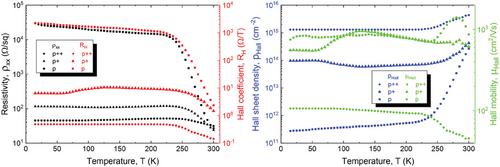
Efficient p- and n-type in situ doping of compressively strained germanium tin (Ge1-xSnx) semiconductor epilayers, grown by chemical vapor deposition on a standard Si(001) substrate, is demonstrated. Materials characterization results reveal unusual impact of dopants manifesting via a pronounced reduction of Sn content in the epilayer, accompanied by an enhancement of the growth rate, due to increasing p-type doping concentration. Furthermore, the opposite behavior for n-type doping is observed, resulting in a less pronounced increase of Sn concentration and no effect on growth rate. Nevertheless, a very high density of electrically active holes up to ≈4 × 1020 cm−3 is obtained in p-type doped Ge1-xSnx epilayer resulting in the lowest resistivity of 0.15 mΩ cm among all in situ doped epitaxial and strained group-IV semiconductors. Also, the metal-to-insulator transition in Ge1-xSnx is experimentally demonstrated for doping levels above 1 × 1017 cm−3, which is substantially lower than in any group-IV semiconductor, and theoretically predict it to be as low as ≈1 × 1017 cm−3. The findings enabled by the doping regime explored in this work can open novel prospects to engineer low resistivity contacts and charge current injection in applications covering next-generation transistors, qubits, diodes, electrically driven light sources, sensors and hybrid quantum devices.
期刊介绍:
Advanced Electronic Materials is an interdisciplinary forum for peer-reviewed, high-quality, high-impact research in the fields of materials science, physics, and engineering of electronic and magnetic materials. It includes research on physics and physical properties of electronic and magnetic materials, spintronics, electronics, device physics and engineering, micro- and nano-electromechanical systems, and organic electronics, in addition to fundamental research.
 求助内容:
求助内容: 应助结果提醒方式:


