{"title":"用于互连器件形成的减法和半减法过程的钌","authors":"A. Rogozhin, A. Miakonkikh, K. Rudenko","doi":"10.1134/s1063739723600851","DOIUrl":null,"url":null,"abstract":"<h3 data-test=\"abstract-sub-heading\">Abstract</h3><p>Ruthenium thin films were deposited by plasma enhanced atomic layer deposition (PEALD) using Ru(EtCp)<sub>2</sub> and oxygen plasma on the modified silicon surface and SiO<sub>2</sub>/Si substrates. The substrate temperature has a significant impact on film growth. The GXRD and SIMS analysis have shown that at the substrate temperature <i>T</i> = 375°C there is a sharp change in the mechanisms of surface reactions, which leads to a change in the film composition from RuO<sub>2</sub> at low temperatures to a pure Ru film at higher temperatures. This was confirmed by measurements of the electrical resistivity of Ru-based films. The lowest surface roughness ~1.5 nm was obtained at a film thickness of 29 nm deposited at 375°C on a SiO<sub>2</sub>/Si-substrate. The measured resistivity of the Ru film was 18–19 μΩ cm. Issues regarding the plasma-chemical etching of ruthenium and the spin-on of a low-k dielectric onto arrays of lines are taken into account.</p>","PeriodicalId":21534,"journal":{"name":"Russian Microelectronics","volume":"148 1","pages":""},"PeriodicalIF":0.0000,"publicationDate":"2024-03-21","publicationTypes":"Journal Article","fieldsOfStudy":null,"isOpenAccess":false,"openAccessPdf":"","citationCount":"0","resultStr":"{\"title\":\"Ruthenium for Subtractive and Semi-Damascene Processes of Interconnects Formation\",\"authors\":\"A. Rogozhin, A. Miakonkikh, K. Rudenko\",\"doi\":\"10.1134/s1063739723600851\",\"DOIUrl\":null,\"url\":null,\"abstract\":\"<h3 data-test=\\\"abstract-sub-heading\\\">Abstract</h3><p>Ruthenium thin films were deposited by plasma enhanced atomic layer deposition (PEALD) using Ru(EtCp)<sub>2</sub> and oxygen plasma on the modified silicon surface and SiO<sub>2</sub>/Si substrates. The substrate temperature has a significant impact on film growth. The GXRD and SIMS analysis have shown that at the substrate temperature <i>T</i> = 375°C there is a sharp change in the mechanisms of surface reactions, which leads to a change in the film composition from RuO<sub>2</sub> at low temperatures to a pure Ru film at higher temperatures. This was confirmed by measurements of the electrical resistivity of Ru-based films. The lowest surface roughness ~1.5 nm was obtained at a film thickness of 29 nm deposited at 375°C on a SiO<sub>2</sub>/Si-substrate. The measured resistivity of the Ru film was 18–19 μΩ cm. Issues regarding the plasma-chemical etching of ruthenium and the spin-on of a low-k dielectric onto arrays of lines are taken into account.</p>\",\"PeriodicalId\":21534,\"journal\":{\"name\":\"Russian Microelectronics\",\"volume\":\"148 1\",\"pages\":\"\"},\"PeriodicalIF\":0.0000,\"publicationDate\":\"2024-03-21\",\"publicationTypes\":\"Journal Article\",\"fieldsOfStudy\":null,\"isOpenAccess\":false,\"openAccessPdf\":\"\",\"citationCount\":\"0\",\"resultStr\":null,\"platform\":\"Semanticscholar\",\"paperid\":null,\"PeriodicalName\":\"Russian Microelectronics\",\"FirstCategoryId\":\"1085\",\"ListUrlMain\":\"https://doi.org/10.1134/s1063739723600851\",\"RegionNum\":0,\"RegionCategory\":null,\"ArticlePicture\":[],\"TitleCN\":null,\"AbstractTextCN\":null,\"PMCID\":null,\"EPubDate\":\"\",\"PubModel\":\"\",\"JCR\":\"Q4\",\"JCRName\":\"Engineering\",\"Score\":null,\"Total\":0}","platform":"Semanticscholar","paperid":null,"PeriodicalName":"Russian Microelectronics","FirstCategoryId":"1085","ListUrlMain":"https://doi.org/10.1134/s1063739723600851","RegionNum":0,"RegionCategory":null,"ArticlePicture":[],"TitleCN":null,"AbstractTextCN":null,"PMCID":null,"EPubDate":"","PubModel":"","JCR":"Q4","JCRName":"Engineering","Score":null,"Total":0}
Ruthenium for Subtractive and Semi-Damascene Processes of Interconnects Formation
Abstract
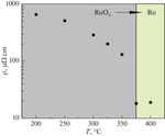
Ruthenium thin films were deposited by plasma enhanced atomic layer deposition (PEALD) using Ru(EtCp)2 and oxygen plasma on the modified silicon surface and SiO2/Si substrates. The substrate temperature has a significant impact on film growth. The GXRD and SIMS analysis have shown that at the substrate temperature T = 375°C there is a sharp change in the mechanisms of surface reactions, which leads to a change in the film composition from RuO2 at low temperatures to a pure Ru film at higher temperatures. This was confirmed by measurements of the electrical resistivity of Ru-based films. The lowest surface roughness ~1.5 nm was obtained at a film thickness of 29 nm deposited at 375°C on a SiO2/Si-substrate. The measured resistivity of the Ru film was 18–19 μΩ cm. Issues regarding the plasma-chemical etching of ruthenium and the spin-on of a low-k dielectric onto arrays of lines are taken into account.
期刊介绍:
Russian Microelectronics covers physical, technological, and some VLSI and ULSI circuit-technical aspects of microelectronics and nanoelectronics; it informs the reader of new trends in submicron optical, x-ray, electron, and ion-beam lithography technology; dry processing techniques, etching, doping; and deposition and planarization technology. Significant space is devoted to problems arising in the application of proton, electron, and ion beams, plasma, etc. Consideration is given to new equipment, including cluster tools and control in situ and submicron CMOS, bipolar, and BICMOS technologies. The journal publishes papers addressing problems of molecular beam epitaxy and related processes; heterojunction devices and integrated circuits; the technology and devices of nanoelectronics; and the fabrication of nanometer scale devices, including new device structures, quantum-effect devices, and superconducting devices. The reader will find papers containing news of the diagnostics of surfaces and microelectronic structures, the modeling of technological processes and devices in micro- and nanoelectronics, including nanotransistors, and solid state qubits.
 求助内容:
求助内容: 应助结果提醒方式:


