{"title":"利用标准 CMOS 技术设计集成电压倍增器","authors":"A. S. Sinyukin, B. G. Konoplev, A. V. Kovalev","doi":"10.1134/s1063739723700713","DOIUrl":null,"url":null,"abstract":"<h3 data-test=\"abstract-sub-heading\">Abstract</h3><p>The results of the design of integrated multistage voltage multipliers as components of supply modules for wireless passive microdevices are presented. The parameters of transistors that are significant for the construction of multipliers are considered for three typical CMOS technologies: CM018G 180 nm, HCMOS8D 180 nm, and C250G 250 nm. The Cadence CAD simulation results demonstrate that when implementing an eight-stage multiplier using the CM018G technology, the minimum output voltage level required for operation of the microcircuit is achieved at input amplitude of 250 mV; and when implementing a similar device using the HCMOS8D technology, at an amplitude of 375 mV. Using the example of the constructed 16-stage multiplier, it is shown that the voltage multiplication efficiency values range from 20 to 54% for a wide range of the input voltage, and the efficiency decreases only by 1–3% compared to the 8-stage implementation. The proposed recommendations for the design of integrated voltage rectifiers-multipliers can be used in the development of the passive supply units for microelectronic devices.</p>","PeriodicalId":21534,"journal":{"name":"Russian Microelectronics","volume":"10 1","pages":""},"PeriodicalIF":0.0000,"publicationDate":"2024-02-08","publicationTypes":"Journal Article","fieldsOfStudy":null,"isOpenAccess":false,"openAccessPdf":"","citationCount":"0","resultStr":"{\"title\":\"Design of Integrated Voltage Multipliers Using Standard CMOS Technologies\",\"authors\":\"A. S. Sinyukin, B. G. Konoplev, A. V. Kovalev\",\"doi\":\"10.1134/s1063739723700713\",\"DOIUrl\":null,\"url\":null,\"abstract\":\"<h3 data-test=\\\"abstract-sub-heading\\\">Abstract</h3><p>The results of the design of integrated multistage voltage multipliers as components of supply modules for wireless passive microdevices are presented. The parameters of transistors that are significant for the construction of multipliers are considered for three typical CMOS technologies: CM018G 180 nm, HCMOS8D 180 nm, and C250G 250 nm. The Cadence CAD simulation results demonstrate that when implementing an eight-stage multiplier using the CM018G technology, the minimum output voltage level required for operation of the microcircuit is achieved at input amplitude of 250 mV; and when implementing a similar device using the HCMOS8D technology, at an amplitude of 375 mV. Using the example of the constructed 16-stage multiplier, it is shown that the voltage multiplication efficiency values range from 20 to 54% for a wide range of the input voltage, and the efficiency decreases only by 1–3% compared to the 8-stage implementation. The proposed recommendations for the design of integrated voltage rectifiers-multipliers can be used in the development of the passive supply units for microelectronic devices.</p>\",\"PeriodicalId\":21534,\"journal\":{\"name\":\"Russian Microelectronics\",\"volume\":\"10 1\",\"pages\":\"\"},\"PeriodicalIF\":0.0000,\"publicationDate\":\"2024-02-08\",\"publicationTypes\":\"Journal Article\",\"fieldsOfStudy\":null,\"isOpenAccess\":false,\"openAccessPdf\":\"\",\"citationCount\":\"0\",\"resultStr\":null,\"platform\":\"Semanticscholar\",\"paperid\":null,\"PeriodicalName\":\"Russian Microelectronics\",\"FirstCategoryId\":\"1085\",\"ListUrlMain\":\"https://doi.org/10.1134/s1063739723700713\",\"RegionNum\":0,\"RegionCategory\":null,\"ArticlePicture\":[],\"TitleCN\":null,\"AbstractTextCN\":null,\"PMCID\":null,\"EPubDate\":\"\",\"PubModel\":\"\",\"JCR\":\"Q4\",\"JCRName\":\"Engineering\",\"Score\":null,\"Total\":0}","platform":"Semanticscholar","paperid":null,"PeriodicalName":"Russian Microelectronics","FirstCategoryId":"1085","ListUrlMain":"https://doi.org/10.1134/s1063739723700713","RegionNum":0,"RegionCategory":null,"ArticlePicture":[],"TitleCN":null,"AbstractTextCN":null,"PMCID":null,"EPubDate":"","PubModel":"","JCR":"Q4","JCRName":"Engineering","Score":null,"Total":0}
Design of Integrated Voltage Multipliers Using Standard CMOS Technologies
Abstract
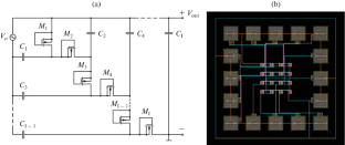
The results of the design of integrated multistage voltage multipliers as components of supply modules for wireless passive microdevices are presented. The parameters of transistors that are significant for the construction of multipliers are considered for three typical CMOS technologies: CM018G 180 nm, HCMOS8D 180 nm, and C250G 250 nm. The Cadence CAD simulation results demonstrate that when implementing an eight-stage multiplier using the CM018G technology, the minimum output voltage level required for operation of the microcircuit is achieved at input amplitude of 250 mV; and when implementing a similar device using the HCMOS8D technology, at an amplitude of 375 mV. Using the example of the constructed 16-stage multiplier, it is shown that the voltage multiplication efficiency values range from 20 to 54% for a wide range of the input voltage, and the efficiency decreases only by 1–3% compared to the 8-stage implementation. The proposed recommendations for the design of integrated voltage rectifiers-multipliers can be used in the development of the passive supply units for microelectronic devices.
期刊介绍:
Russian Microelectronics covers physical, technological, and some VLSI and ULSI circuit-technical aspects of microelectronics and nanoelectronics; it informs the reader of new trends in submicron optical, x-ray, electron, and ion-beam lithography technology; dry processing techniques, etching, doping; and deposition and planarization technology. Significant space is devoted to problems arising in the application of proton, electron, and ion beams, plasma, etc. Consideration is given to new equipment, including cluster tools and control in situ and submicron CMOS, bipolar, and BICMOS technologies. The journal publishes papers addressing problems of molecular beam epitaxy and related processes; heterojunction devices and integrated circuits; the technology and devices of nanoelectronics; and the fabrication of nanometer scale devices, including new device structures, quantum-effect devices, and superconducting devices. The reader will find papers containing news of the diagnostics of surfaces and microelectronic structures, the modeling of technological processes and devices in micro- and nanoelectronics, including nanotransistors, and solid state qubits.
 求助内容:
求助内容: 应助结果提醒方式:


