{"title":"带浮动电极的微机电系统开关的性能计算","authors":"M. O. Morozov, I. V. Uvarov","doi":"10.1134/s1063739723700750","DOIUrl":null,"url":null,"abstract":"<h3 data-test=\"abstract-sub-heading\">Abstract</h3><p>Switches fabricated using MEMS technology are considered as a promising element base of radio electronics. The main characteristic of a MEMS switch is the ratio of capacitances in the closed and open states. For conventional devices, this ratio is of several units, but it can be significantly increased by implementing original design solutions. This paper studies the switch, which is a combination of capacitive and resistive devices. Its working characteristics are considered depending on the substrate properties and contact resistance. The switch provides a capacitance ratio of 27.7 and 46.1 when using sapphire and borosilicate glass substrates, while high-resistivity silicon does not allow attaining values above 7.4 due to the high parasitic capacitance. The isolation and insertion loss are 14.7–19.4 and 0.8–1.1 dB in the frequency range of 4–10 GHz on a sapphire wafer. Acceptable S-parameters are achieved when the contact resistance is not higher than 1 Ω.</p>","PeriodicalId":21534,"journal":{"name":"Russian Microelectronics","volume":"2 1","pages":""},"PeriodicalIF":0.0000,"publicationDate":"2024-02-08","publicationTypes":"Journal Article","fieldsOfStudy":null,"isOpenAccess":false,"openAccessPdf":"","citationCount":"0","resultStr":"{\"title\":\"Performance Calculation for a MEMS Switch with a Floating Electrode\",\"authors\":\"M. O. Morozov, I. V. Uvarov\",\"doi\":\"10.1134/s1063739723700750\",\"DOIUrl\":null,\"url\":null,\"abstract\":\"<h3 data-test=\\\"abstract-sub-heading\\\">Abstract</h3><p>Switches fabricated using MEMS technology are considered as a promising element base of radio electronics. The main characteristic of a MEMS switch is the ratio of capacitances in the closed and open states. For conventional devices, this ratio is of several units, but it can be significantly increased by implementing original design solutions. This paper studies the switch, which is a combination of capacitive and resistive devices. Its working characteristics are considered depending on the substrate properties and contact resistance. The switch provides a capacitance ratio of 27.7 and 46.1 when using sapphire and borosilicate glass substrates, while high-resistivity silicon does not allow attaining values above 7.4 due to the high parasitic capacitance. The isolation and insertion loss are 14.7–19.4 and 0.8–1.1 dB in the frequency range of 4–10 GHz on a sapphire wafer. Acceptable S-parameters are achieved when the contact resistance is not higher than 1 Ω.</p>\",\"PeriodicalId\":21534,\"journal\":{\"name\":\"Russian Microelectronics\",\"volume\":\"2 1\",\"pages\":\"\"},\"PeriodicalIF\":0.0000,\"publicationDate\":\"2024-02-08\",\"publicationTypes\":\"Journal Article\",\"fieldsOfStudy\":null,\"isOpenAccess\":false,\"openAccessPdf\":\"\",\"citationCount\":\"0\",\"resultStr\":null,\"platform\":\"Semanticscholar\",\"paperid\":null,\"PeriodicalName\":\"Russian Microelectronics\",\"FirstCategoryId\":\"1085\",\"ListUrlMain\":\"https://doi.org/10.1134/s1063739723700750\",\"RegionNum\":0,\"RegionCategory\":null,\"ArticlePicture\":[],\"TitleCN\":null,\"AbstractTextCN\":null,\"PMCID\":null,\"EPubDate\":\"\",\"PubModel\":\"\",\"JCR\":\"Q4\",\"JCRName\":\"Engineering\",\"Score\":null,\"Total\":0}","platform":"Semanticscholar","paperid":null,"PeriodicalName":"Russian Microelectronics","FirstCategoryId":"1085","ListUrlMain":"https://doi.org/10.1134/s1063739723700750","RegionNum":0,"RegionCategory":null,"ArticlePicture":[],"TitleCN":null,"AbstractTextCN":null,"PMCID":null,"EPubDate":"","PubModel":"","JCR":"Q4","JCRName":"Engineering","Score":null,"Total":0}
Performance Calculation for a MEMS Switch with a Floating Electrode
Abstract
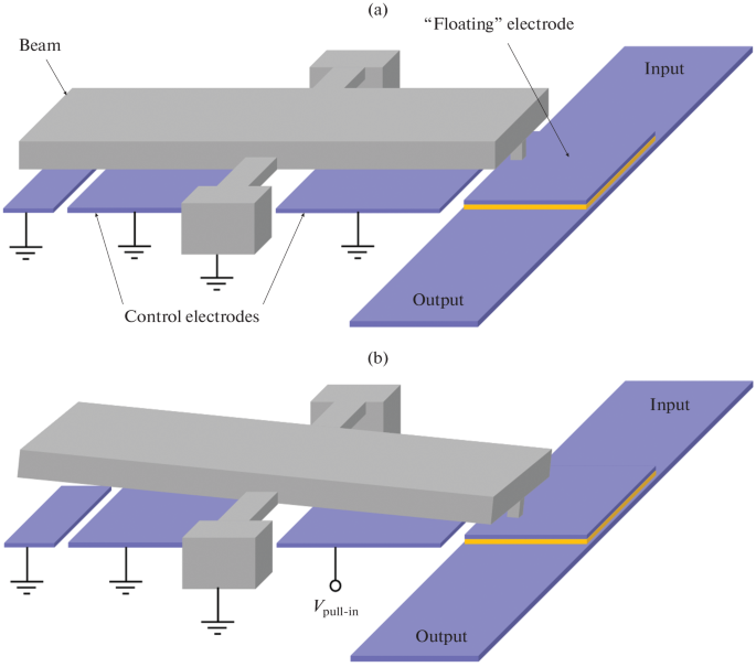
Switches fabricated using MEMS technology are considered as a promising element base of radio electronics. The main characteristic of a MEMS switch is the ratio of capacitances in the closed and open states. For conventional devices, this ratio is of several units, but it can be significantly increased by implementing original design solutions. This paper studies the switch, which is a combination of capacitive and resistive devices. Its working characteristics are considered depending on the substrate properties and contact resistance. The switch provides a capacitance ratio of 27.7 and 46.1 when using sapphire and borosilicate glass substrates, while high-resistivity silicon does not allow attaining values above 7.4 due to the high parasitic capacitance. The isolation and insertion loss are 14.7–19.4 and 0.8–1.1 dB in the frequency range of 4–10 GHz on a sapphire wafer. Acceptable S-parameters are achieved when the contact resistance is not higher than 1 Ω.
期刊介绍:
Russian Microelectronics covers physical, technological, and some VLSI and ULSI circuit-technical aspects of microelectronics and nanoelectronics; it informs the reader of new trends in submicron optical, x-ray, electron, and ion-beam lithography technology; dry processing techniques, etching, doping; and deposition and planarization technology. Significant space is devoted to problems arising in the application of proton, electron, and ion beams, plasma, etc. Consideration is given to new equipment, including cluster tools and control in situ and submicron CMOS, bipolar, and BICMOS technologies. The journal publishes papers addressing problems of molecular beam epitaxy and related processes; heterojunction devices and integrated circuits; the technology and devices of nanoelectronics; and the fabrication of nanometer scale devices, including new device structures, quantum-effect devices, and superconducting devices. The reader will find papers containing news of the diagnostics of surfaces and microelectronic structures, the modeling of technological processes and devices in micro- and nanoelectronics, including nanotransistors, and solid state qubits.
 求助内容:
求助内容: 应助结果提醒方式:


