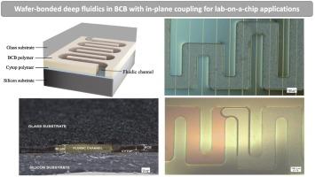
Wafer-bonded deep fluidics in BCB with in-plane coupling for lab-on-a-chip applications

IF 2.8 Q2 ENGINEERING, ELECTRICAL & ELECTRONIC
Deepthi Sekhar , Ewa Lisicka-Skrzek , Pierre Berini
{"title":"Wafer-bonded deep fluidics in BCB with in-plane coupling for lab-on-a-chip applications","authors":"Deepthi Sekhar ,&nbsp;Ewa Lisicka-Skrzek ,&nbsp;Pierre Berini","doi":"10.1016/j.mne.2023.100227","DOIUrl":null,"url":null,"abstract":"<div><p>The wafer-scale fabrication of deep channel microfluidics for lab-on-a-chip applications by reactive ion etching and wafer bonding is reported. The microfluidic channels are etched in B-stage bisbenzocyclobutene (BCB) and Cytop with the latter used as a bonding agent. The channels are hermetically sealed between Borofloat glass and Si wafers by wafer bonding. Fluidic coupling is achieved in the plane of the channels via inlets and outlets that are revealed on the end facets of chips after dicing. Process techniques and details are reported for uniform coating and curing of BCB and Cytop, defining the channels with high accuracy using photolithography, dry etching the polymers using a hard mask, and sealing the channels by wafer bonding. Fluidic measurements are carried out at various flow rates and compared with modeling. The low Reynold's numbers of the channels ensure laminar flow conditions. Deep fluidic channels are less difficult to align to fluidic interfaces, they support higher flow rates and are less susceptible to clogging. In-plane fluidic coupling precludes the need to etch holes through the substrate. Our wafer-scale process was applied to 4 in. diameter wafers yielding 195 precision-aligned and hermetically sealed microfluidic chips, but is readily scalable to larger diameter wafers for volume production.</p></div>","PeriodicalId":37111,"journal":{"name":"Micro and Nano Engineering","volume":"21 ","pages":"Article 100227"},"PeriodicalIF":2.8000,"publicationDate":"2023-09-21","publicationTypes":"Journal Article","fieldsOfStudy":null,"isOpenAccess":false,"openAccessPdf":"","citationCount":"0","resultStr":null,"platform":"Semanticscholar","paperid":null,"PeriodicalName":"Micro and Nano Engineering","FirstCategoryId":"1085","ListUrlMain":"https://www.sciencedirect.com/science/article/pii/S2590007223000576","RegionNum":0,"RegionCategory":null,"ArticlePicture":[],"TitleCN":null,"AbstractTextCN":null,"PMCID":null,"EPubDate":"","PubModel":"","JCR":"Q2","JCRName":"ENGINEERING, ELECTRICAL & ELECTRONIC","Score":null,"Total":0}
引用次数: 0

Abstract

The wafer-scale fabrication of deep channel microfluidics for lab-on-a-chip applications by reactive ion etching and wafer bonding is reported. The microfluidic channels are etched in B-stage bisbenzocyclobutene (BCB) and Cytop with the latter used as a bonding agent. The channels are hermetically sealed between Borofloat glass and Si wafers by wafer bonding. Fluidic coupling is achieved in the plane of the channels via inlets and outlets that are revealed on the end facets of chips after dicing. Process techniques and details are reported for uniform coating and curing of BCB and Cytop, defining the channels with high accuracy using photolithography, dry etching the polymers using a hard mask, and sealing the channels by wafer bonding. Fluidic measurements are carried out at various flow rates and compared with modeling. The low Reynold's numbers of the channels ensure laminar flow conditions. Deep fluidic channels are less difficult to align to fluidic interfaces, they support higher flow rates and are less susceptible to clogging. In-plane fluidic coupling precludes the need to etch holes through the substrate. Our wafer-scale process was applied to 4 in. diameter wafers yielding 195 precision-aligned and hermetically sealed microfluidic chips, but is readily scalable to larger diameter wafers for volume production.
Abstract Image

用于芯片实验室应用的BCB中具有平面内耦合的晶片键合深流体
报道了通过反应离子蚀刻和晶片键合在晶片规模上制备用于芯片实验室应用的深通道微流体。微流体通道在B阶段双苯并环丁烯(BCB)和Cytop中蚀刻,后者用作结合剂。通道通过晶片键合密封在硼浮法玻璃和硅晶片之间。流体耦合在通道的平面中通过入口和出口实现,所述入口和出口在划片后显示在芯片的端面上。报道了BCB和Cytop的均匀涂覆和固化的工艺技术和细节,使用光刻法高精度地定义通道,使用硬掩模干法蚀刻聚合物,并通过晶片键合密封通道。流体测量在不同的流速下进行,并与建模进行比较。雷诺数较低的通道确保了层流条件。深层流体通道不太难与流体界面对齐,它们支持更高的流速,并且不太容易堵塞。平面内流体耦合排除了蚀刻穿过衬底的孔的需要。我们的晶圆级工艺应用于4英寸。直径晶片产生195个精确对准和密封的微流体芯片,但易于扩展到用于批量生产的较大直径晶片。
本文章由计算机程序翻译,如有差异,请以英文原文为准。
求助全文
约1分钟内获得全文 求助全文
来源期刊
Micro and Nano Engineering
Micro and Nano Engineering Engineering-Electrical and Electronic Engineering
CiteScore
3.30
自引率
0.00%
发文量
67
审稿时长
80 days
×
引用
GB/T 7714-2015
复制
MLA
复制
APA
复制
导出至
BibTeX EndNote RefMan NoteFirst NoteExpress
×
提示
您的信息不完整,为了账户安全,请先补充。
现在去补充
×
提示
您因"违规操作"
具体请查看互助需知
我知道了
×
提示
确定
请完成安全验证×
copy
已复制链接
快去分享给好友吧!
我知道了
右上角分享
点击右上角分享
0
联系我们:info@booksci.cn Book学术提供免费学术资源搜索服务,方便国内外学者检索中英文文献。致力于提供最便捷和优质的服务体验。 Copyright © 2023 布克学术 All rights reserved.
京ICP备2023020795号-1
ghs 京公网安备 11010802042870号
Book学术文献互助
Book学术文献互助群
群 号:481959085
Book学术官方微信