Hierarchical copper nanostructures synthesized on microparticles for improved photothermal conversion in photonic sintering of copper-based printed electrodes†
IF 5.1 2区 材料科学Q2 MATERIALS SCIENCE, MULTIDISCIPLINARY
Jae-Won Lee, Juhee Kim, Ji Hye Kwak, Jung Hoon Kim, Sooyeon Jeong, Joong Tark Han, Geon-Woong Lee, Kang-Jun Baeg, Kyong-Soo Hong, Imjeong H.-S. Yang and Hee Jin Jeong
{"title":"Hierarchical copper nanostructures synthesized on microparticles for improved photothermal conversion in photonic sintering of copper-based printed electrodes†","authors":"Jae-Won Lee, Juhee Kim, Ji Hye Kwak, Jung Hoon Kim, Sooyeon Jeong, Joong Tark Han, Geon-Woong Lee, Kang-Jun Baeg, Kyong-Soo Hong, Imjeong H.-S. Yang and Hee Jin Jeong","doi":"10.1039/D2TC03645B","DOIUrl":null,"url":null,"abstract":"<p >Photonic sintering of Cu-particle-based printed patterns using intense pulsed light (IPL) is a promising route to the large-scale fabrication of printed electronics for commercial applications. Despite the significant advantages of photonic sintering, which include the process being ultrafast, extremely low-cost, and eco-friendly, realizing a high-conductivity Cu-printed electrode remains a major challenge. In particular, low light absorption caused by the low surface plasmon density of Cu particles is the origin of insufficient temperature increase even after IPL irradiation. In this study, hierarchical nanostructured (HN) Cu microparticles (Cu μPs) with improved light absorption ability and lower surface melting point were prepared for the fabrication of high-conductivity Cu electrodes by using IPL sintering. HN-Cu μPs of uniform size were synthesized using a wet chemical hydrothermal method, with Cu(<small>II</small>) nitrate trihydrate, ethylenediamine (EDA), and Cu μPs as the precursor, structure-directing agent, and template, respectively. The morphology of the hierarchical nanostructures could be readily tuned by varying the synthesis time and the amounts of the precursor and EDA. On the basis of ultraviolet-visible spectroscopy, X-ray diffraction, and temperature measurements, the enhanced light absorption in the visible wavelength range was ascribed to the increase in the surface plasmon density of the hierarchical Cu nanostructures. After photonic sintering, the HN-Cu μP-based printed patterns showed highly dense Cu morphologies, which resulted in an extremely low electrical resistivity of 16 μΩ cm for IPL with an energy density of 7 J cm<small><sup>?2</sup></small>.</p>","PeriodicalId":84,"journal":{"name":"Journal of Materials Chemistry C","volume":" 45","pages":" 17336-17342"},"PeriodicalIF":5.1000,"publicationDate":"2022-11-14","publicationTypes":"Journal Article","fieldsOfStudy":null,"isOpenAccess":false,"openAccessPdf":"","citationCount":"0","resultStr":null,"platform":"Semanticscholar","paperid":null,"PeriodicalName":"Journal of Materials Chemistry C","FirstCategoryId":"1","ListUrlMain":"https://pubs.rsc.org/en/content/articlelanding/2022/tc/d2tc03645b","RegionNum":2,"RegionCategory":"材料科学","ArticlePicture":[],"TitleCN":null,"AbstractTextCN":null,"PMCID":null,"EPubDate":"","PubModel":"","JCR":"Q2","JCRName":"MATERIALS SCIENCE, MULTIDISCIPLINARY","Score":null,"Total":0}
引用次数: 0
Abstract
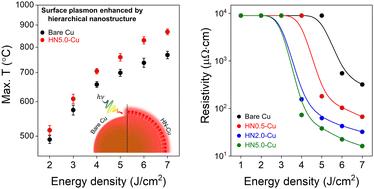
Photonic sintering of Cu-particle-based printed patterns using intense pulsed light (IPL) is a promising route to the large-scale fabrication of printed electronics for commercial applications. Despite the significant advantages of photonic sintering, which include the process being ultrafast, extremely low-cost, and eco-friendly, realizing a high-conductivity Cu-printed electrode remains a major challenge. In particular, low light absorption caused by the low surface plasmon density of Cu particles is the origin of insufficient temperature increase even after IPL irradiation. In this study, hierarchical nanostructured (HN) Cu microparticles (Cu μPs) with improved light absorption ability and lower surface melting point were prepared for the fabrication of high-conductivity Cu electrodes by using IPL sintering. HN-Cu μPs of uniform size were synthesized using a wet chemical hydrothermal method, with Cu(II) nitrate trihydrate, ethylenediamine (EDA), and Cu μPs as the precursor, structure-directing agent, and template, respectively. The morphology of the hierarchical nanostructures could be readily tuned by varying the synthesis time and the amounts of the precursor and EDA. On the basis of ultraviolet-visible spectroscopy, X-ray diffraction, and temperature measurements, the enhanced light absorption in the visible wavelength range was ascribed to the increase in the surface plasmon density of the hierarchical Cu nanostructures. After photonic sintering, the HN-Cu μP-based printed patterns showed highly dense Cu morphologies, which resulted in an extremely low electrical resistivity of 16 μΩ cm for IPL with an energy density of 7 J cm?2.
期刊介绍:
The Journal of Materials Chemistry is divided into three distinct sections, A, B, and C, each catering to specific applications of the materials under study:
Journal of Materials Chemistry A focuses primarily on materials intended for applications in energy and sustainability.
Journal of Materials Chemistry B specializes in materials designed for applications in biology and medicine.
Journal of Materials Chemistry C is dedicated to materials suitable for applications in optical, magnetic, and electronic devices.
Example topic areas within the scope of Journal of Materials Chemistry C are listed below. This list is neither exhaustive nor exclusive.
Bioelectronics
Conductors
Detectors
Dielectrics
Displays
Ferroelectrics
Lasers
LEDs
Lighting
Liquid crystals
Memory
Metamaterials
Multiferroics
Photonics
Photovoltaics
Semiconductors
Sensors
Single molecule conductors
Spintronics
Superconductors
Thermoelectrics
Topological insulators
Transistors

 求助内容:
求助内容: 应助结果提醒方式:


