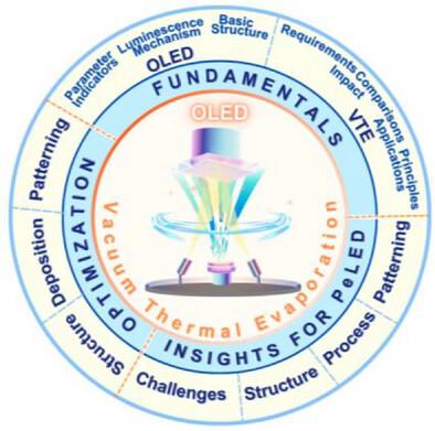
Vacuum Thermal Evaporation for OLEDs: Fundamentals, Optimization, and Implications for Perovskite LEDs
IF 5.3
2区 材料科学
Q2 MATERIALS SCIENCE, MULTIDISCIPLINARY
引用次数: 0
Abstract
Organic light‐emitting diodes (OLEDs) are central to high‐end displays and solid‐state lighting due to their small thickness and high flexibility, wide color gamut, and low power consumption. While solution processing offers simplicity and cost advantages for polymer‐based OLEDs, vacuum thermal evaporation (VTE) remains the dominant method for the commercial production of high‐performance small‐molecule OLEDs, owing to its precise control over film thickness, material purity, and multilayer integration. However, to meet the demands of display applications for higher performance, lower cost and more diverse forms (such as flexibility and high resolution), it is crucial to continuously optimize the VTE process. Meanwhile, although solution processing remains the predominant approach for perovskite light‐emitting diodes (PeLEDs), recent exploratory efforts have investigated VTE as an alternative route, thereby opening opportunities to transfer process insights from OLEDs to PeLEDs. This review aims to systematically summarize the application foundation and optimization strategies of VTE technology in OLEDs, and to explore how these mature practices can inform the process development and device design of vacuum‐evaporated PeLEDs.
有机发光二极管的真空热蒸发:基本原理、优化和钙钛矿led的影响
有机发光二极管(oled)因其厚度小、灵活性高、色域宽、功耗低而成为高端显示器和固态照明的核心。虽然溶液工艺为聚合物基oled提供了简单和成本优势,但真空热蒸发(VTE)仍然是商业生产高性能小分子oled的主要方法,因为它可以精确控制薄膜厚度、材料纯度和多层集成。然而,为了满足显示应用对更高性能、更低成本和更多样化形式(如灵活性和高分辨率)的需求,不断优化VTE工艺至关重要。与此同时,尽管溶液处理仍然是钙钛矿发光二极管(pled)的主要方法,但最近的探索性工作已经将VTE作为一种替代途径进行了研究,从而开辟了将工艺见解从oled转移到pled的机会。本文旨在系统地总结真空蒸发发光二极管技术在oled中的应用基础和优化策略,并探讨这些成熟的实践如何指导真空蒸发发光二极管的工艺开发和器件设计。
本文章由计算机程序翻译,如有差异,请以英文原文为准。
求助全文
约1分钟内获得全文
求助全文
来源期刊

Advanced Electronic Materials
NANOSCIENCE & NANOTECHNOLOGYMATERIALS SCIE-MATERIALS SCIENCE, MULTIDISCIPLINARY
CiteScore
11.00
自引率
3.20%
发文量
433
期刊介绍:
Advanced Electronic Materials is an interdisciplinary forum for peer-reviewed, high-quality, high-impact research in the fields of materials science, physics, and engineering of electronic and magnetic materials. It includes research on physics and physical properties of electronic and magnetic materials, spintronics, electronics, device physics and engineering, micro- and nano-electromechanical systems, and organic electronics, in addition to fundamental research.
 求助内容:
求助内容: 应助结果提醒方式:


