Yonglin Yang, Xiao Fu, Honglong Ning, Zhihao Liang, Weixin Cheng, Junxiong Luo, Han He, Weiguang Xie, Rihui Yao and Junbiao Peng
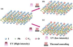
{"title":"Enhanced charge trapping effect in PVA/PbI2 synaptic transistors achieved through integrated UV irradiation and thermal annealing treatments","authors":"Yonglin Yang, Xiao Fu, Honglong Ning, Zhihao Liang, Weixin Cheng, Junxiong Luo, Han He, Weiguang Xie, Rihui Yao and Junbiao Peng","doi":"10.1039/D5TC01587A","DOIUrl":null,"url":null,"abstract":"<p >Charge-trapping synaptic transistors, owing to their excellent non-volatility, controllable channel conductance, and switching performance, have garnered widespread attention as promising candidates for neuromorphic devices. In this study, the underlying PVA film can smooth the surface of the PbI<small><sub>2</sub></small> film, thus decreasing its surface roughness and alleviating the charge trapping phenomenon at the PbI<small><sub>2</sub></small>/IGZO heterojunction. The PVA/PbI<small><sub>2</sub></small> charge-trapping synaptic transistors exhibit progressively enhanced charge-trapping capacity with increasing PbI<small><sub>2</sub></small> thickness, attributed to the elevated concentration of iodine vacancies (V<small><sub>I</sub></small>) within the PbI<small><sub>2</sub></small> layer. Moreover, the synergistic combination of UV irradiation and thermal annealing can significantly enhance the charge trapping capability of PVA/PbI<small><sub>2</sub></small> synaptic transistors because it induces the decomposition of PbI<small><sub>2</sub></small> and the formation of PbO, thus modulating the concentration of V<small><sub>I</sub></small>. At a lower UV irradiation intensity of 87.5 mW cm<small><sup>−2</sup></small>, the hysteresis window of the devices initially increases, then decreases with increasing temperature. In contrast, when the UV irradiation intensity is elevated to 122.5 mW cm<small><sup>−2</sup></small>, the hysteresis window shows a monotonic decrease with increasing temperature. When the UV irradiation intensity was maintained at 87.5 mW cm<small><sup>−2</sup></small> and the thermal annealing temperature at 150 °C, the device demonstrated a substantial hysteresis window of 8.56 ± 0.34 V (<em>V</em><small><sub>G</sub></small>: −10–10 V). Finally, the PVA/PbI<small><sub>2</sub></small> charge-trapping synaptic transistor manifested typical synaptic characteristics. The image recognition accuracy reached as high as 90.1% after 40 training epochs. This suggests that PVA/PbI<small><sub>2</sub></small> synaptic transistors hold considerable promise in the fields of neuromorphic computing and artificial intelligence (AI).</p>","PeriodicalId":84,"journal":{"name":"Journal of Materials Chemistry C","volume":" 39","pages":" 20169-20181"},"PeriodicalIF":5.1000,"publicationDate":"2025-09-09","publicationTypes":"Journal Article","fieldsOfStudy":null,"isOpenAccess":false,"openAccessPdf":"","citationCount":"0","resultStr":null,"platform":"Semanticscholar","paperid":null,"PeriodicalName":"Journal of Materials Chemistry C","FirstCategoryId":"1","ListUrlMain":"https://pubs.rsc.org/en/content/articlelanding/2025/tc/d5tc01587a","RegionNum":2,"RegionCategory":"材料科学","ArticlePicture":[],"TitleCN":null,"AbstractTextCN":null,"PMCID":null,"EPubDate":"","PubModel":"","JCR":"Q2","JCRName":"MATERIALS SCIENCE, MULTIDISCIPLINARY","Score":null,"Total":0}
引用次数: 0
Abstract
Charge-trapping synaptic transistors, owing to their excellent non-volatility, controllable channel conductance, and switching performance, have garnered widespread attention as promising candidates for neuromorphic devices. In this study, the underlying PVA film can smooth the surface of the PbI2 film, thus decreasing its surface roughness and alleviating the charge trapping phenomenon at the PbI2/IGZO heterojunction. The PVA/PbI2 charge-trapping synaptic transistors exhibit progressively enhanced charge-trapping capacity with increasing PbI2 thickness, attributed to the elevated concentration of iodine vacancies (VI) within the PbI2 layer. Moreover, the synergistic combination of UV irradiation and thermal annealing can significantly enhance the charge trapping capability of PVA/PbI2 synaptic transistors because it induces the decomposition of PbI2 and the formation of PbO, thus modulating the concentration of VI. At a lower UV irradiation intensity of 87.5 mW cm−2, the hysteresis window of the devices initially increases, then decreases with increasing temperature. In contrast, when the UV irradiation intensity is elevated to 122.5 mW cm−2, the hysteresis window shows a monotonic decrease with increasing temperature. When the UV irradiation intensity was maintained at 87.5 mW cm−2 and the thermal annealing temperature at 150 °C, the device demonstrated a substantial hysteresis window of 8.56 ± 0.34 V (VG: −10–10 V). Finally, the PVA/PbI2 charge-trapping synaptic transistor manifested typical synaptic characteristics. The image recognition accuracy reached as high as 90.1% after 40 training epochs. This suggests that PVA/PbI2 synaptic transistors hold considerable promise in the fields of neuromorphic computing and artificial intelligence (AI).
期刊介绍:
The Journal of Materials Chemistry is divided into three distinct sections, A, B, and C, each catering to specific applications of the materials under study:
Journal of Materials Chemistry A focuses primarily on materials intended for applications in energy and sustainability.
Journal of Materials Chemistry B specializes in materials designed for applications in biology and medicine.
Journal of Materials Chemistry C is dedicated to materials suitable for applications in optical, magnetic, and electronic devices.
Example topic areas within the scope of Journal of Materials Chemistry C are listed below. This list is neither exhaustive nor exclusive.
Bioelectronics
Conductors
Detectors
Dielectrics
Displays
Ferroelectrics
Lasers
LEDs
Lighting
Liquid crystals
Memory
Metamaterials
Multiferroics
Photonics
Photovoltaics
Semiconductors
Sensors
Single molecule conductors
Spintronics
Superconductors
Thermoelectrics
Topological insulators
Transistors

 求助内容:
求助内容: 应助结果提醒方式:


