{"title":"Quantification of interfacial trap states via bias-applied HAXPES: a chemical-state perspective","authors":"Wen-Jen Chen, Yin-Bo Tseng and Hsiu-Wei Cheng","doi":"10.1039/D5TC01375E","DOIUrl":null,"url":null,"abstract":"<p >An interface where two solid materials meet often disrupts bulk continuity, especially in electronic structures. When an external bias is applied, the interfacial electronic structure forms a voltage barrier that inhibits charge transfer and promotes charge accumulation—a key mechanism in semiconductor devices. However, our understanding of such interfaces remains limited at the molecular scale. Here, we quantitatively characterize interfacial trap states in a model Si|SiO<small><sub>2</sub></small>|Au MOS structure using bias-applied hard X-ray photoelectron spectroscopy (BA-HAXPES), resolving oxidation state variations across the dielectric layer under real-time bias. While conventional interpretations rely on peak shifts to describe charging effects, our results demonstrate that these shifts are also sensitive to dielectric thickness and local potential variations; thus, we propose a modified Grahame-based framework to contextualize the influence of interfacial potential on chemical-state changes and to support the use of peak intensity as a more reliable indicator. Furthermore, bias-dependent analysis reveals distinct charge dynamics for different oxidation states: Si<small><sup>3+</sup></small> exhibits potential-driven delocalization behavior, resembling mobile carriers within the dielectric, whereas Si<small><sup>2+</sup></small> remains strongly confined to the SiO<small><sub>2</sub></small>|Au interface, acting as a localized trap signature. These trends are consistently observed across the full bias range and provide a more direct connection between chemical state evolution and interfacial trap-state activity. Our findings offer molecular-level insight into charge accumulation mechanisms and support future trap-state engineering in nanoscale electronic devices.</p>","PeriodicalId":84,"journal":{"name":"Journal of Materials Chemistry C","volume":" 38","pages":" 19856-19866"},"PeriodicalIF":5.1000,"publicationDate":"2025-09-04","publicationTypes":"Journal Article","fieldsOfStudy":null,"isOpenAccess":false,"openAccessPdf":"","citationCount":"0","resultStr":null,"platform":"Semanticscholar","paperid":null,"PeriodicalName":"Journal of Materials Chemistry C","FirstCategoryId":"1","ListUrlMain":"https://pubs.rsc.org/en/content/articlelanding/2025/tc/d5tc01375e","RegionNum":2,"RegionCategory":"材料科学","ArticlePicture":[],"TitleCN":null,"AbstractTextCN":null,"PMCID":null,"EPubDate":"","PubModel":"","JCR":"Q2","JCRName":"MATERIALS SCIENCE, MULTIDISCIPLINARY","Score":null,"Total":0}
引用次数: 0
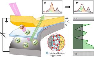
Abstract
An interface where two solid materials meet often disrupts bulk continuity, especially in electronic structures. When an external bias is applied, the interfacial electronic structure forms a voltage barrier that inhibits charge transfer and promotes charge accumulation—a key mechanism in semiconductor devices. However, our understanding of such interfaces remains limited at the molecular scale. Here, we quantitatively characterize interfacial trap states in a model Si|SiO2|Au MOS structure using bias-applied hard X-ray photoelectron spectroscopy (BA-HAXPES), resolving oxidation state variations across the dielectric layer under real-time bias. While conventional interpretations rely on peak shifts to describe charging effects, our results demonstrate that these shifts are also sensitive to dielectric thickness and local potential variations; thus, we propose a modified Grahame-based framework to contextualize the influence of interfacial potential on chemical-state changes and to support the use of peak intensity as a more reliable indicator. Furthermore, bias-dependent analysis reveals distinct charge dynamics for different oxidation states: Si3+ exhibits potential-driven delocalization behavior, resembling mobile carriers within the dielectric, whereas Si2+ remains strongly confined to the SiO2|Au interface, acting as a localized trap signature. These trends are consistently observed across the full bias range and provide a more direct connection between chemical state evolution and interfacial trap-state activity. Our findings offer molecular-level insight into charge accumulation mechanisms and support future trap-state engineering in nanoscale electronic devices.
期刊介绍:
The Journal of Materials Chemistry is divided into three distinct sections, A, B, and C, each catering to specific applications of the materials under study:
Journal of Materials Chemistry A focuses primarily on materials intended for applications in energy and sustainability.
Journal of Materials Chemistry B specializes in materials designed for applications in biology and medicine.
Journal of Materials Chemistry C is dedicated to materials suitable for applications in optical, magnetic, and electronic devices.
Example topic areas within the scope of Journal of Materials Chemistry C are listed below. This list is neither exhaustive nor exclusive.
Bioelectronics
Conductors
Detectors
Dielectrics
Displays
Ferroelectrics
Lasers
LEDs
Lighting
Liquid crystals
Memory
Metamaterials
Multiferroics
Photonics
Photovoltaics
Semiconductors
Sensors
Single molecule conductors
Spintronics
Superconductors
Thermoelectrics
Topological insulators
Transistors

 求助内容:
求助内容: 应助结果提醒方式:


