Nonequilibrium Nitrogen Spike Annealing for Crystallization Enhancement Achieves High Mobility and Reliability in IGO TFTs
IF 5.3
2区 材料科学
Q2 MATERIALS SCIENCE, MULTIDISCIPLINARY
引用次数: 0
Abstract
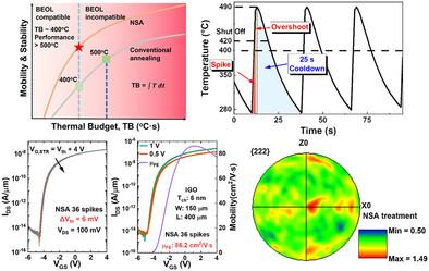
Poly-crystallized In-Ga-O (IGO) semiconductor has the potential for application in high-density memory and back end of line (BEOL) integration with CPU. Since the development of In2O3-based multi-cation oxides, i.e., IGZO, such material is very difficult to be poly-crystallized under the limitation of BEOL temperature. Here, a novel Nitrogen-Spike Annealing (NSA) method is demonstrated, this nonequilibrium annealing process utilizes a transient high temperature to induce crystallization while reducing the overall thermal budget. During NSA, the O atoms are more intended to bond with Ga, resulting in a more rigid framework that stabilizes the O atoms. The crystal orientation of the NSA treated IGO film is more concentrated compared with the conventional equilibrium annealed one. Furthermore, poly-IGO thin-film transistors (TFTs) with high crystallinity and more centered crystal orientation are demonstrated through material characterization. Electrical characteristics revealed that the poly-IGO TFT exhibits high mobility of ≈86.2 cm2 V s−1 and enhanced reliability after NSA treatment. These findings will advance the design and improvement of oxide semiconductor memory applications.
非平衡态氮峰退火晶化增强实现了高迁移率和高可靠性
多晶in - ga - o (IGO)半导体在高密度存储器和与CPU的后端集成(BEOL)方面具有潜在的应用前景。由于基于in2o3的多阳离子氧化物即IGZO的发展,这种材料在BEOL温度的限制下很难多晶化。本文提出了一种新的氮峰退火(NSA)方法,这种非平衡退火工艺利用瞬态高温诱导结晶,同时减少了整体热收支。在NSA过程中,O原子更倾向于与Ga结合,从而形成一个更坚固的框架来稳定O原子。经过NSA处理的IGO薄膜的晶体取向比常规平衡退火的IGO薄膜更加集中。此外,通过材料表征,证明了具有高结晶度和更中心取向的多igo薄膜晶体管(TFTs)。电学特性表明,经过NSA处理后,聚igo TFT具有≈86.2 cm2 V s−1的高迁移率和增强的可靠性。这些发现将推动氧化物半导体存储器应用的设计和改进。
本文章由计算机程序翻译,如有差异,请以英文原文为准。
求助全文
约1分钟内获得全文
求助全文
来源期刊

Advanced Electronic Materials
NANOSCIENCE & NANOTECHNOLOGYMATERIALS SCIE-MATERIALS SCIENCE, MULTIDISCIPLINARY
CiteScore
11.00
自引率
3.20%
发文量
433
期刊介绍:
Advanced Electronic Materials is an interdisciplinary forum for peer-reviewed, high-quality, high-impact research in the fields of materials science, physics, and engineering of electronic and magnetic materials. It includes research on physics and physical properties of electronic and magnetic materials, spintronics, electronics, device physics and engineering, micro- and nano-electromechanical systems, and organic electronics, in addition to fundamental research.
 求助内容:
求助内容: 应助结果提醒方式:


